
Daquan Yang, Xiao Liu, Xiaogang Li, Bing Duan, Aiqiang Wang, Yunfeng Xiao. Photoic crystal nanobeam cavity devices for on-chip integrated silicon photonics[J]. Journal of Semiconductors, 2021, 42(2): 023103
- Journal of Semiconductors
- Vol. 42, Issue 2, 023103 (2021)
Abstract
1. Introduction
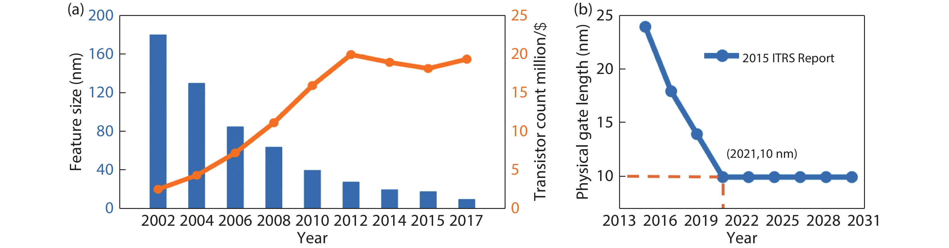
Over the past few decades, the mainstream of integrated circuit (IC) industry has been mainly powered by Moore’s Law, which is targeted at achieving faster operation speed, less power dissipation, and lower cost[
![]()
Figure 3.(Color online) A summary of PCNC lasers (2010–2018). Insets show the device structures, materials, and threshold power, respectively.
In fact, Moore’s Law is a techno-economic model that has enabled the information technology industry to double the performance and functionality of digital electronics roughly every two years within a fixed cost, power, and area[
![]()
Figure 5.(Color online) (a) Schematic of the proposed room temperature, suspended silicon nanobeam laser with a monolayer MoTe2 on top. The corresponding lasing spectra of the nanobeam laser under different pump power levels (b) using a grating resolution: 150 g/mm (0.41 nm), and (c) using a grating resolution: 600 g/mm (0.09 nm).
Silicon photonics have been widely investigated in recent years, which benefits from academic research efforts and available commercial complementary metal–oxide–semiconductor (CMOS) process for potential mass-production applications[
Particularly, photonic crystal nanobeam cavity (PCNC) is considered as an ideal platform for on-chip integration, due to the advantages of an ultracompact footprint, enhanced light–matter interactions, high integrability with optical waveguides/circuits, and compatibility with CMOS processes[
2. On-chip PCNC devices for lasing
Photonic crystal lasers, with large Q/V, have enhanced photon emission below threshold through the Purcell effect, and can operate at a higher modulation speed[
![]()
Figure 7.(Color online) (a) SEM image of the proposed parallel quadrabeam PCNCs. (b) Real-time monitoring of streptavidin/biotin binding. Inset: resonance shift as a function of streptavidin concentration in PBS. (c) Resonance shifts as a function of the refractive indices with different concentrations ethanol/water solutions. (d) SEM of nanoscale sensor array. (e) Red shift of the targeted resonator occurs because of the higher refractive index of the CaCl2 solution. (f) Experimental data showing the redshifts for various refractive index solutions.
For example, Lee et al. demonstrated an ultracompact nanobeam laser by effectively integrating a wavelength-scale unidirectional III−V materials onto a SOI waveguide[
Monolayer transition-metal dichalcogenides (TMDs) exhibit great potential to be the smallest and efficient optical gain media for low energy-consumption nanolasers due to its strong excitonic emission[
3. On-chip PCNC devices for modulation
Silicon photonics technology is poised to resolve short reach interconnects, and optical modulators are essential for such an interconnect. In addition, Pockels effect[
Several parameters have been used to characterize the performance of EO modulator: footprint, modulation voltage, modulation speed, extinction ratio, and energy consumption. So far, various silicon hybrid EO modulators have been achieved. But for waveguide-based modulators, they have large footprints and high-power consumptions due to the interaction lengths about several tens of micrometers[
We can find that many works based on the combination of PCNC and new materials have been reported[
4. On-chip PCNC devices for switching/filting
Optical switch is widely used in optical communication[
PCNCs are increasingly gaining interest in optical switch due to the advantages of high Q/V. Therefore, it could be an effective method in realizing low power-consumption optical switches. For comparison, Table 2 summarizes the performances of some PCNC-based optical switches. For thermo-optic (TO) switch, Su et al. proposed and experimentally demonstrated a 2 × 2 TO crossbar switch based on dual-PCNCs[
With the advancement of photonic integration technology, the filters have drawn much attention due to highly energy-efficient tunability[
5. On-chip PCNC devices for label-free sensing
Ultra-sensitive and label-free detection of the analyte plays an important part in the field of homeland security, environment protection and medical diagnostics[
Hence, most research has focused on the optimization of PCNCs design to improve sensitivity, as shown in Table 3. With the rapid development of technology, micro-nano devices are moving towards high miniaturization and integration. Much research has been proposed for label-free sensing by integrating microfluidics with PCNCs. For instance, Yang et al. presented a nanoslotted parallel quadrabeam photonic crystal cavity sensor, with high sensitivity of 451 nm/RIU and high-Q of 7015 in aqueous environments at wavelength of 1550 nm[
In conclusion, with the rapid development of silicon photonics devices, higher integration, and miniaturization are required. Among these, PCNCs are considered as candidates for on-chip label-free sensing and multiple channel sensing, due to the advantages of an ultra-small footprint, ultrahigh Q/V, and excellent CMOS compatibility properties[
6. Summary
To be implemented in practice, technical challenges are existed in manufacturing. The silicon photonics chip can be fabricated cost-effectively with CMOS-compatible technology. However, the fabrication tolerance limits the practical applications of PCNCs, which makes them impractical for high-yield production. Fabrication tolerance in the position and size of the PhC structures may result in fluctuations of resonance wavelength and Q factor[
In this paper, we review recent advances on photonics devices for lasers, modulators, switches/filters, and sensors based on PCNCs. It has been shown that PCNCs with ultrahigh Q/V, ultrasmall footprint are an idea platform for the monolithic integration and extending the capability of these optical devices, in which the key is that the PCNCs can greatly improve light-matter interaction. The optical devices show good characteristics and high-volume production, which are expected to benefit large-scale photonic-integrated circuits on silicon in the near future. Furthermore, photonic integration should not be required to surpass electronic integration, but its unique advantages should be used as a supplement to electronic integration to solve problems that electronic integration cannot solve in the More-than-Moore era.
Acknowledgements
This work was supported by the National Key R&D Program of China (Grant No. 2016YFA0301302 and No. 2018YFB2200401), the National Natural Science Foundation of China (Grant Nos. 11974058, 11825402, 11654003, 61435001), Beijing Academy of Quantum Information Sciences (Grant No. Y18G20), Key R&D Program of Guangdong Province (Grant No. 2018B030329001), Beijing Nova Program (Grant No. Z201100006820125) from Beijing Municipal Science and Technology Commission, Fundamental Research Funds for the Central Universities (Grant No. 2018XKJC05) and the High Performance Computing Platform of Peking University.
References
[1] J M Shalf, R Leland. Computing beyond Moore's law. Computer, 48, 14(2015).
[2] M S Liu, Y Liu, H J Wang et al. Design of GeSn-based heterojunction-enhanced N-channel tunneling FET with improved subthreshold swing and ON-state current. IEEE Trans Electron Devices, 62, 1262(2015).
[3] Y Z Yue, Y Hao, J C Zhang et al. AlGaN/GaN MOS-HEMT with HfO2 dielectric and Al2O3 interfacial passivation layer grown by atomic layer deposition. IEEE Electron Device Lett, 29, 838(2008).
[4] I L Markov. Limits on fundamental limits to computation. Nature, 512, 147(2014).
[5] P Wesling. The Heterogeneous integration roadmap: Enabling technology for systems of the future. 2020 Pan Pacific Microelectronics Symposium (Pan Pacific), 1(2020).
[6] J Shalf. The future of computing beyond Moore's Law. Phil Trans Royal Soc A, 378, 20190061(2020).
[7] J Pei, L Deng, S Song et al. Towards artificial general intelligence with hybrid Tianjic chip architecture. Nature, 572, 106(2019).
[8] W L Liu, M Li, R S Guzzon et al. A fully reconfigurable photonic integrated signal processor. Nat Photon, 10, 190(2016).
[9] D Thomson, A Zilkie, J E Bowers et al. Roadmap on silicon photonics. J Opt, 18, 073003(2016).
[10] D X Dai, Y L Yin, L H Yu et al. Silicon-plus photonics. Front Optoelectron, 9, 436(2016).
[11] Y C Shi, J Y Chen, H N Xu. Silicon-based on-chip diplexing/triplexing technologies and devices. Sci China Inf Sci, 61, 080402(2018).
[12] J S Guo, D X Dai. Silicon nanophotonics for on-chip light manipulation. Chin Phys B, 27, 104208(2018).
[13] H S Rong, S B Xu, Y H Kuo et al. Low-threshold continuous-wave Raman silicon laser. Nat Photon, 1, 232(2007).
[14] X C Sun, J F Liu, L C Kimerling et al. Toward a germanium laser for integrated silicon photonics. IEEE J Sel Top Quantum Electron, 16, 124(2010).
[15] G H Duan, C Jany, A Le Liepvre et al. Hybrid III–V on silicon lasers for photonic integrated circuits on silicon. IEEE J Sel Top Quantum Electron, 20, 158(2014).
[16] Y C Yang, P Gao, L Z Li et al. Electrochemical dynamics of nanoscale metallic inclusions in dielectrics. Nat Commun, 5, 4232(2014).
[17] F Pyatkov, V Fütterling, S Khasminskaya et al. Cavity-enhanced light emission from electrically driven carbon nanotubes. Nat Photon, 10, 420(2016).
[18] B G Chen, H Wu, C G Xin et al. Flexible integration of free-standing nanowires into silicon photonics. Nat Commun, 8, 20(2017).
[19] J L Liu, G M Xu, F G Liu et al. Recent advances in polymer electro-optic modulators. RSC Adv, 5, 15784(2015).
[20] H J Joyce, Q Gao, H Hoe Tan et al. III –V semiconductor nanowires for optoelectronic device applications. Prog Quantum Electron, 35, 23(2011).
[21] Y Q Bie, G Grosso, M Heuck et al. A MoTe2-based light-emitting diode and photodetector for silicon photonic integrated circuits. Nat Nanotech, 12, 1124(2017).
[22] M Liu, X B Yin, E Ulin-Avila et al. A graphene-based broadband optical modulator. Nature, 474, 64(2011).
[23] K J Vahala. Optical microcavities. Nature, 424, 839(2003).
[24] Q H Song. Emerging opportunities for ultra-high
[25] P B Deotare, M W McCutcheon, I W Frank et al. High quality factor photonic crystal nanobeam cavities. Appl Phys Lett, 94, 121106(2009).
[26] Q M Quan, P B Deotare, M Loncar. Photonic crystal nanobeam cavity strongly coupled to the feeding waveguide. Appl Phys Lett, 96, 203102(2010).
[27] Y Zhang, M Khan, Y Huang et al. Photonic crystal nanobeam lasers. Appl Phys Lett, 97, 051104(2010).
[28] B H Ahn, J H Kang, M K Kim et al. One-dimensional parabolic-beam photonic crystal laser. Opt Express, 18, 5654(2010).
[29] Y Y Gong, B Ellis, G Shambat et al. Nanobeam photonic crystal cavity quantum dot laser. Opt Express, 18, 8781(2010).
[30] T W Lu, L H Chiu, P T Lin et al. One-dimensional photonic crystal nanobeam lasers on a flexible substrate. Appl Phys Lett, 99, 071101(2011).
[31] W S Fegadolli, S H Kim, P A Postigo et al. Hybrid single quantum well InP/Si nanobeam lasers for silicon photonics. Opt Lett, 38, 4656(2013).
[32] P T Lee, T W Lu, L H Chiu. Dielectric-band photonic crystal nanobeam lasers. J Lightwave Technol, 31, 36(2013).
[33] K Y Jeong, Y S No, Y Hwang et al. Electrically driven nanobeam laser. Nat Commun, 4, 2822(2013).
[34] N Niu, A Woolf, D Q Wang et al. Ultra-low threshold gallium nitride photonic crystal nanobeam laser. Appl Phys Lett, 106, 231104(2015).
[35] N V Triviño, R Butté, J F Carlin et al. Continuous wave blue lasing in III-nitride nanobeam cavity on silicon. Nano Lett, 15, 1259(2015).
[36] Z L Yang, M Pelton, I Fedin et al. A room temperature continuous-wave nanolaser using colloidal quantum wells. Nat Commun, 8, 143(2017).
[37] J Lee, I Karnadi, J T Kim et al. Printed nanolaser on silicon. ACS Photonics, 4, 2117(2017).
[38] Y Z Li, J X Zhang, D D Huang et al. Room-temperature continuous-wave lasing from monolayer molybdenum ditelluride integrated with a silicon nanobeam cavity. Nat Nanotech, 12, 987(2017).
[39] S T Jagsch, N V Triviño, F Lohof et al. A quantum optical study of thresholdless lasing features in high-
[40] Z He, B Chen, Y Hua et al. CMOS compatible high-performance nanolasing based on perovskite-SiN hybrid integration. Adv Opt Mater, 8, 2000453(2020).
[41] S F Wu, S Buckley, J R Schaibley et al. Monolayer semiconductor nanocavity lasers with ultralow thresholds. Nature, 520, 69(2015).
[42] R S Jacobsen, K N Andersen, P I Borel et al. Strained silicon as a new electro-optic material. Nature, 441, 199(2006).
[43] M Hochberg, T Baehr-Jones, G X Wang et al. Terahertz all-optical modulation in a silicon–polymer hybrid system. Nat Mater, 5, 703(2006).
[44] R Soref, B Bennett. Electrooptical effects in silicon. IEEE J Quantum Electron, 23, 123(1987).
[45] B Qi, P Yu, Y B Li et al. Analysis of electrooptic modulator with 1-D slotted photonic crystal nanobeam cavity. IEEE Photon Technol Lett, 23, 992(2011).
[46] M R Javid, M Miri, A Zarifkar. Design of a compact high-speed optical modulator based on a hybrid plasmonic nanobeam cavity. Opt Commun, 410, 652(2018).
[47] J Hendrickson, R Soref, J Sweet et al. Ultrasensitive silicon photonic-crystal nanobeam electro-optical modulator: Design and simulation. Opt Express, 22, 3271(2014).
[48] A Shakoor, K Nozaki, E Kuramochi et al. Compact 1D-silicon photonic crystal electro-optic modulator operating with ultra-low switching voltage and energy. Opt Express, 22, 28623(2014).
[49] Z Jafari, A Zarifkar, M Miri et al. All-optical modulation in a graphene-covered slotted silicon nano-beam cavity. J Lightwave Technol, 36, 4051(2018).
[50] M Liu, X B Yin, X Zhang. Double-layer graphene optical modulator. Nano Lett, 12, 1482(2012).
[51] C Y Qiu, W L Gao, R Vajtai et al. Efficient modulation of 1.55
[52] W Du, E P Li, R Hao. Tunability analysis of a graphene-embedded ring modulator. IEEE Photon Technol Lett, 26, 2008(2014).
[53] T Pan, C Y Qiu, J Y Wu et al. Analysis of an electro-optic modulator based on a graphene-silicon hybrid 1D photonic crystal nanobeam cavity. Opt Express, 23, 23357(2015).
[54] H Q Liu, P G Liu, L A Bian et al. Electro-optic modulator side-coupled with a photonic crystal nanobeam loaded graphene/ Al2O3 multilayer stack. Opt Mater Express, 8, 761(2018).
[55] S I Inoue, A Otomo. Electro-optic polymer/silicon hybrid slow light modulator based on one-dimensional photonic crystal waveguides. Appl Phys Lett, 103, 171101(2013).
[56] H Yan, X C Xu, C J Chung et al. One-dimensional photonic crystal slot waveguide for silicon-organic hybrid electro-optic modulators. Opt Lett, 41, 5466(2016).
[57] J D Witmer, J T Hill, A H Safavi-Naeini. Design of nanobeam photonic crystal resonators for a silicon-on-lithium-niobate platform. Opt Express, 24, 5876(2016).
[58] J D Witmer, J A Valery, P Arrangoiz-Arriola et al. High-
[59] W S Fegadolli, J E B Oliveira, V R Almeida et al. Compact and low power consumption tunable photonic crystal nanobeam cavity. Opt Express, 21, 3861(2013).
[60] B Hadian Siahkal-Mahalle, K Abedi. Ultra-compact low loss electro-optical nanobeam cavity modulator embedded photonic crystal. Opt Quant Electron, 51, 128(2019).
[61] K I Bolotin, K J Sikes, Z Jiang et al. Ultrahigh electron mobility in suspended graphene. Solid State Commun, 146, 351(2008).
[62] K F Mak, M Y Sfeir, Y Wu et al. Measurement of the optical conductivity of graphene. Phys Rev Lett, 101, 196405(2008).
[63] Y W Yin, R Proietti, X H Ye et al. LIONS: An AWGR-based low-latency optical switch for high-performance computing and data centers. IEEE J Sel Top Quantum Electron, 19, 3600409(2013).
[64] K Chen, A Singla, A Singh et al. OSA: an optical switching architecture for data center networks with unprecedented flexibility. IEEE/ACM Trans Networking, 22, 498(2014).
[65] C Y Qiu, W L Gao, R Soref et al. Reconfigurable electro-optical directed-logic circuit using carrier-depletion micro-ring resonators. Opt Lett, 39, 6767(2014).
[66] H L R Lira, S Manipatruni, M Lipson. Broadband hitless silicon electro-optic switch for on-chip optical networks. Opt Express, 17, 22271(2009).
[67] P Dong, S R Liao, H Liang et al. Submilliwatt, ultrafast and broadband electro-optic silicon switches. Opt Express, 18, 25225(2010).
[68] H Y Zhou, C Y Qiu, Z Z Xu et al. A 2 × 2 silicon thermo-optic switch based on nanobeam cavities with ultra-small mode volumes. 2016 IEEE 13th International Conference on Group IV Photonics (GFP), 10(2016).
[69] H Y Zhou, C Y Qiu, X H Jiang et al. Compact, submilliwatt, 2 × 2 silicon thermo-optic switch based on photonic crystal nanobeam cavities. Photon Res, 5, 108(2017).
[70] Z W Cheng, J J Dong, X L Zhang. Ultracompact optical switch using a single semisymmetric Fano nanobeam cavity. Opt Lett, 45, 2363(2020).
[71] R Soref, J Hendrickson. Proposed ultralow-energy dual photonic-crystal nanobeam devices for on-chip
[72] R Soref, J R Hendrickson, J Sweet. Simulation of germanium nanobeam electro-optical 2 × 2 switches and 1 × 1 modulators for the 2 to 5
[73] H Y Zhou, C Y Qiu, J Y Wu et al. 2 × 2 electro-optic switch with fJ/bit switching power based on dual photonic crystal nanobeam cavities. Conference on Lasers and Electro-Optics, JTh2A.105(2016).
[74] A Bazin, K Lenglé, M Gay et al. Ultrafast all-optical switching and error-free 10 Gbit/s wavelength conversion in hybrid InP-silicon on insulator nanocavities using surface quantum wells. Appl Phys Lett, 104, 011102(2014).
[75] G N Dong, W T Deng, J Hou et al. Ultra-compact multi-channel all-optical switches with improved switching dynamic characteristics. Opt Express, 26, 25630(2018).
[76] Z M Meng, C B Chen, F Qin. Theoretical investigation of integratable photonic crystal nanobeam all-optical switching with ultrafast response and ultralow switching energy. J Phys D, 53, 205105(2020).
[77] Y Liu, F Qin, Z M Meng et al. All-optical logic gates based on two-dimensional low-refractive-index nonlinear photonic crystal slabs. Opt Express, 19, 1945(2011).
[78] K Lengle, T N Nguyen, M Gay et al. Modulation contrast optimization for wavelength conversion of a 20 Gbit/s data signal in hybrid InP/SOI photonic crystal nanocavity. Opt Lett, 39, 2298(2014).
[79] H Ji, M Galili, H Hu et al. 1.28-Tb/s demultiplexing of an OTDM DPSK data signal using a silicon waveguide. IEEE Photon Technol Lett, 22, 1762(2010).
[80] G N Dong, Y L Wang, X L Zhang. High-contrast and low-power all-optical switch using Fano resonance based on a silicon nanobeam cavity. Opt Lett, 43, 5977(2018).
[81] Z M Meng, Y H Hu, C Wang et al. Design of high-
[82] M Asghari, A V Krishnamoorthy. Energy-efficient communication. Nat Photon, 5, 268(2011).
[83] J Pan, Y J Huo, K Yamanaka et al. Aligning microcavity resonances in silicon photonic-crystal slabs using laser-pumped thermal tuning. Appl Phys Lett, 92, 103114(2008).
[84] M Eichenfield, R Camacho, J Chan et al. A picogram- and nanometre-scale photonic-crystal optomechanical cavity. Nature, 459, 550(2009).
[85] M Li, W H P Pernice, H X Tang. Tunable bipolar optical interactions between guided lightwaves. Nat Photon, 3, 464(2009).
[86] L L Gu, W Jiang, X N Chen et al. Thermooptically tuned photonic crystal waveguide silicon-on-insulator Mach–Zehnder interferometers. IEEE Photon Technol Lett, 19, 342(2007).
[87] R L Espinola, M C Tsai, J T Yardley et al. Fast and low-power thermooptic switch on thin silicon-on-insulator. IEEE Photon Technol Lett, 15, 1366(2003).
[88] P Dong, W Qian, H Liang et al. Thermally tunable silicon racetrack resonators with ultralow tuning power. Opt Express, 18, 20298(2010).
[89] Y Zhang, Y He, Q M Zhu et al. Single-resonance silicon nanobeam filter with an ultra-high thermo-optic tuning efficiency over a wide continuous tuning range. Opt Lett, 43, 4518(2018).
[90]
[91]
[92] A Sharma, S R Xie, R Zeltner et al. On-the-fly particle metrology in hollow-core photonic crystal fibre. Opt Express, 27, 34496(2019).
[93] Y F Xiao, Q H Gong. Optical microcavity: From fundamental physics to functional photonics devices. Sci Bull, 61, 185(2016).
[94] Y Y Zhi, X C Yu, Q H Gong et al. Single nanoparticle detection using optical microcavities. Adv Mater, 29, 1604920(2017).
[95] L B Shao, X F Jiang, X C Yu et al. Detection of single nanoparticles and lentiviruses using microcavity resonance broadening. Adv Mater, 25, 5616(2013).
[96] B B Li, W R Clements, X C Yu et al. Single nanoparticle detection using split-mode microcavity Raman lasers. PNAS, 111, 14657(2014).
[97] D Q Yang, A Q Wang, J H Chen et al. Real-time monitoring of hydrogel phase transition in an ultrahigh
[98] D Q Yang, B Duan, X Liu et al. Photonic crystal nanobeam cavities for nanoscale optical sensing: A review. Micromachines, 11, 72(2020).
[99] Q M Quan, D L Floyd, I B Burgess et al. Single particle detection in CMOS compatible photonic crystal nanobeam cavities. Opt Express, 21, 32225(2013).
[100] M G A Rahman, P Velha, R M de la Rue et al. Silicon-on-insulator (SOI) nanobeam optical cavities for refractive index based sensing. Opt Sens Detect II, 8439, 84391Q(2012).
[101] K Y Yao, Y C Shi. High-
[102] Q M Quan, I B Burgess, S K Y Tang et al. High-
[103] P P Xu, K Y Yao, J J Zheng et al. Slotted photonic crystal nanobeam cavity with parabolic modulated width stack for refractive index sensing. Opt Express, 21, 26908(2013).
[104] D Q Yang, S Kita, F Liang et al. High sensitivity and high
[105] S Kim, H M Kim, Y H Lee. Single nanobeam optical sensor with a high
[106] G A Rodriguez, P Markov, A P Cartwright et al. Photonic crystal nanobeam biosensors based on porous silicon. Opt Express, 27, 9536(2019).
[107] A Gopinath, E Miyazono, A Faraon et al. Engineering and mapping nanocavity emission via precision placement of DNA origami. Nature, 535, 401(2016).
[108] S Mandal, D Erickson. Nanoscale optofluidic sensor arrays. Opt Express, 16, 1623(2008).
[109] D Q Yang, C Wang, Y F Ji. Silicon on-chip 1D photonic crystal nanobeam bandstop filters for the parallel multiplexing of ultra-compact integrated sensor array. Opt Express, 24, 16267(2016).
[110] H Hagino, Y Takahashi, Y Tanaka et al. Effects of fluctuation in air hole radii and positions on optical characteristics in photonic crystal heterostructure nanocavities. Phys Rev B, 79, 085112(2009).
[111] F O Afzal, S I Halimi, S M Weiss. Efficient side-coupling to photonic crystal nanobeam cavities via state-space overlap. J Opt Soc Am B, 36, 585(2019).
[112] F Liang, N Clarke, P Patel et al. Scalable photonic crystal chips for high sensitivity protein detection. Opt Express, 21, 32306(2013).
[113] I W Frank, P B Deotare, M W McCutcheon et al. Programmable photonic crystal nanobeam cavities. Opt Express, 18, 8705(2010).
[114] D Panettieri, L O'Faolain, M Grande. Control of
[115] Y L Xiong, J G Wangüemert-Pérez, D X Xu et al. Polarization splitter and rotator with subwavelength grating for enhanced fabrication tolerance. Opt Lett, 39, 6931(2014).


Set citation alerts for the article
Please enter your email address

© Copyright 2018-2021 | Chinese Laser Press. All Rights Reserved 沪ICP备15018463号-20