
Ningqin Deng, He Tian, Jian Zhang, Jinming Jian, Fan Wu, Yang Shen, Yi Yang, Tian-Ling Ren. Black phosphorus junctions and their electrical and optoelectronic applications[J]. Journal of Semiconductors, 2021, 42(8): 081001
- Journal of Semiconductors
- Vol. 42, Issue 8, 081001 (2021)
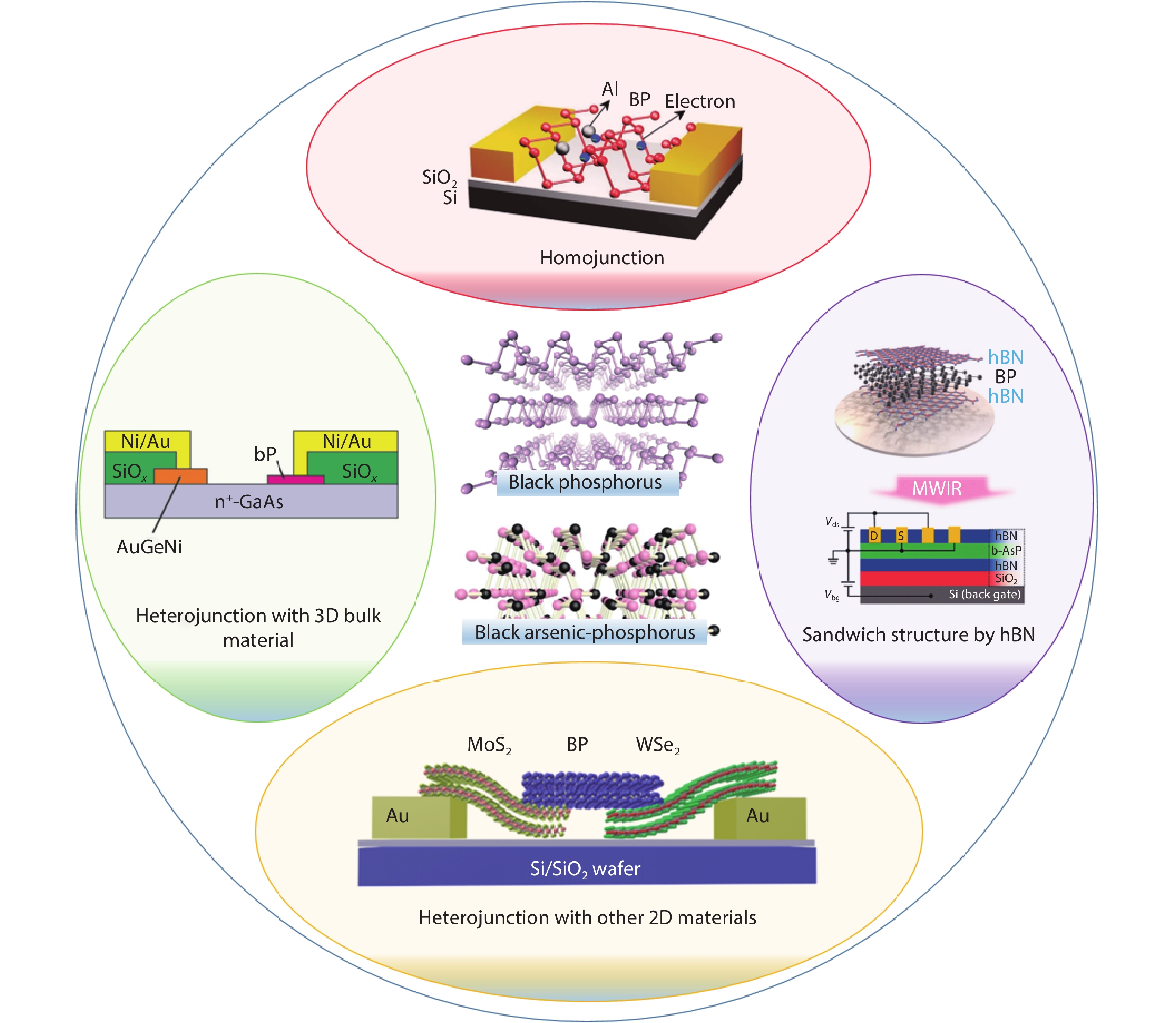
Fig. 1. (Color online) Overview of BP crystal structure and BP devices.
![(Color online) Black phosphorus sandwich structure integration with hBN and its band structure. (a) A 3D schematic of hBN/BP/hBN heterostructure. (b) The HSE06 calculation results of the band structure and the local density of states (LDOS) for the hBN/BP heterostructure. Modified with permission from Ref. [38] Copyright 2016 American Chemical Society, (b) Ref. [39] Copyright 2015 American Chemical Society.](/richHtml/jos/2021/42/8/081001/img_2.jpg)
Fig. 2. (Color online) Black phosphorus sandwich structure integration with hBN and its band structure. (a) A 3D schematic of hBN/BP/hBN heterostructure. (b) The HSE06 calculation results of the band structure and the local density of states (LDOS) for the hBN/BP heterostructure. Modified with permission from Ref. [38 ] Copyright 2016 American Chemical Society, (b) Ref. [39 ] Copyright 2015 American Chemical Society.
Fig. 3. (Color online) Fabrication process and mobility of hBN/BP/hBN heterostructure devices. (a) A 3D schematic of hBN/BP/hBN heterostructure device fabrication process. (b) Mobility results of the different structures including BP/SiO2 (red), BP/hBN (green), and hBN/BP/hBN (blue). (c) Mobility results of the trilayer and 20-layer were measured at liquid helium temperatures. (d) Mobility as a function of temperature for different carrier densities were measured. (e) Quantum Hall states with filling factors from 2 to 12 are observed. (f) FET and Hall mobilities at different temperature. Modified with permission from (a) Ref. [30 ] Copyright Nature publishing group, (b) Ref. [45 ] Copyright AIP Publishing, (c) Ref. [46 ] Copyright 2015 American Chemical Society, (d) and (e) Ref. [47 ] Copyright 2016 American Chemical Society, (f) Ref. [48 ] Copyright 2018 American Chemical Society.
Fig. 4. (Color online) Drain current mapping and band diagrams of the few-layer black phosphorus PN junction. Drain current mapping at (a) + 100 mV and (b) –100 mV as a function of V rg and V Ig, respectively. (c) Schematic energy band diagrams of the different device configurations. Modified with permission from Ref. [65 ] Copyright 2014 Springer Nature.
Fig. 5. (Color online) Bandgap and structure of graphene/BP heterojunction. (a) The top and side views of schematics of BP (violet)/graphene (gray) heterojunction. (b) The HSE06 calculation results of the band structure are graphene, phosphorene and graphene/BP heterojunction, respectively. (c) Transfer characteristic curves for an encapsulated device by measuring under both vacuum and ambient conditions. The inset shows a nonencapsulated device test. (d) Transfer characteristic curves at ranging various temperatures from 300 to 30 K in 30 K steps. Modified with permission from (a) and (b) Ref. [82 ] Copyright Royal Society of Chemistry, (c) Ref. [61 ] Copyright 2015 American Chemical Society, (d) Ref. [64 ] Copyright 2016 American Chemical Society.
Fig. 6. (Color online) The photodetectors based on TMDCs/BP heterojunctions. (a) A 3D schematic of the BP/MoS2 heterojunction device. (b) On/off switching characteristics of the BP/MoS2 junction device under illumination of 1.55 μ m laser (Laser power 96.2 μ W) at different bias voltages. The rise time and the decay were 15 μ s and 70 μ s, respectively. (c) A 3D schematic of the WSe2/BP/MoS2 heterojunction device. (d) Photoresponsivity and photogain of the WSe2/BP/MoS2 heterojunction device as a function of wavelength, respectively. (e) A 3D schematic diagram of the ReS2/BP heterojunction device. (f) Current rectifying output characteristics as a function of incident laser power values under illumination of 532 nm laser. Modified with permission from (a) and (b) Ref. [74 ] Copyright 2016 American Chemical Society, (c) and (d) Ref. [75 ] Copyright 2017 American Chemical Society, (e) and (f) Ref. [76 ] Copyright 2019 American Chemical Society.
Fig. 7. (Color online) Structure and performance of the lateral and vertical BP/MoS2 heterostructures. (a) A 3D schematic of the BP/MoS2 heterojunction device. (b) The diode current (I d) as a function of the voltage across the diode at different thicknesses of BP which are 9, 36 and 61 nm, respectively. (c) A schematic diagram of the BP/MoS2 heterostructure device cross-section. (d) I–V characteristics of vertical and lateral BP/MoS2 heterojunction diodes. The inset shows semilogarithmic scale plot of the same I–V curves. Modified with permission from (a) and (b) Ref. [63 ] Copyright 2017 American Chemical Society, (c) and (d) Ref. [92 ] Copyright 2017 American Chemical Society.
Fig. 8. (Color online) Performance of BP/ 3D bulk material heterojunction device. (a) EQE as a function of laser power for different laser light wavelengths at zero source–drain bias based on BP/GaAs heterojunction. (b) Semi-log plot of the transfer characteristics of the JFET based on BP/β -Ga2O3 heterojunction. (c) The transfer characteristics of BP/InGaZnO JFET. The inset shows the corresponding µ FE value. Modified with permission from (a) Ref. [94 ] Copyright AIP publishing, (b) Ref. [96 ] Copyright 2020 IOP, (c) Ref. [109 ] Copyright 2020 John Wiley and Sons.
Fig. 9. (Color online) Performance of the related b-AsP photodetectors. (a) Infrared absorption as a function of wavenumber for different samples including b-P, b-As0.25P0.75, b-As0.4P0.6 and b-As0.83P0.17, respectively. (b) Bandgap and wavelength as a function of different composition-tunable b-AsxP1−x or different polarization angle of the same composition, respectively. (c) Response curve as a function of time under illumination of 4.034 μ m of the b-AsP photodetector. (d) Specific detectivity of different detectors as a function of wavelength including a thermistor bolometer, a PbSe detector, a b-AsP FET device and a b-AsP/MoS2 heterostructure. Modified with permission from (a) and (b) Ref. [95 ] Copyright John Wiley and Sons, (c) and (d) Ref. [97 ] Copyright AAAS.
|
Table 1. Comparison of performance of FETs based on BP and BP heterostructures, including BP film thickness, structure, mobility, on/off ratio.
|
Table 2. Comparison of performance of photodetectors based on BP and BP-related heterostructures, including film thickness, structure, spectral range, responsivity, specific detectivity and response time.

Set citation alerts for the article
Please enter your email address
© Copyright 2018-2021 | Chinese Laser Press. All Rights Reserved 沪ICP备15018463号-20