• Journal of Semiconductors
  • Vol. 42, Issue 8, 081001 (2021)
Ningqin Deng3, He Tian1、2, Jian Zhang3, Jinming Jian1、2, Fan Wu1、2, Yang Shen1、2, Yi Yang1、2, and Tian-Ling Ren1、2
Author Affiliations
  • 1Institute of Microelectronics, Tsinghua University, Beijing 100084, China
  • 2Beijing National Research Center for Information Science and Technology (BNRist), Tsinghua University, Beijing 100084, China
  • 3National Institute of Metrology (NIM), Beijing 100029, China
  • show less
    DOI: 10.1088/1674-4926/42/8/081001 Cite this Article
    Ningqin Deng, He Tian, Jian Zhang, Jinming Jian, Fan Wu, Yang Shen, Yi Yang, Tian-Ling Ren. Black phosphorus junctions and their electrical and optoelectronic applications[J]. Journal of Semiconductors, 2021, 42(8): 081001 Copy Citation Text show less

    Abstract

    Black phosphorus (BP), an emerging two-dimensional material, is considered a promising candidate for next-generation electronic and optoelectronic devices due to in-plane anisotropy, high mobility, and direct bandgap. However, BP devices face challenges due to their limited stability, photo-response speed, and detection range. To enhance BP with powerful electrical and optical performance, the BP heterostructures can be created. In this review, the state-of-the-art heterostructures and their electrical and optoelectronic applications based on black phosphorus are discussed. Five parts introduce the performance of BP-based devices, including black phosphorus sandwich structure by hBN with better stability and higher mobility, black phosphorus homojunction by dual-gate structure for optical applications, black phosphorus heterojunction with other 2D materials for faster photo-detection, black phosphorus heterojunction integration with 3D bulk material, and BP via As-doping tunable bandgap enabling photo-detection up to 8.2 μm. Finally, we discuss the challenges and prospects for BP electrical and optical devices and applications.

    1. Introduction

    It is well known that the industry based on silicon faces many challenges due to the continuous scaling down the feature size[1-3]. Therefore, breakthroughs in materials science play a significant role in the future development of technology and various applications. In 2004, graphene was the first discovered two-dimensional (2D) material extracted as a single layer of carbon atoms that are bonded together in a hexagonal honeycomb lattice from graphite[4]. It had attracted worldwide attention owing to its unique properties, including ultra-high mobility[5] and thermal conductivity[6], transparency[7], and high Young's modulus[8]. By virtue of their outstanding contribution to graphene development, the graphene discoverers, Konstantin Novoselov and Andre Geim, were awarded the Nobel Prize for physics in 2010. Devices based on graphene have shown various promising applications such as transistors[9-11], supercapacitors[12], batteries[13], solar cells[14], speakers[15, 16], and thermal rectifiers[17], etc. In brief, graphene has blazed a new trail for developing 2D material and has a promising future from research laboratories to industrial applications. However, the on/off ratio of graphene transistors was limited to ~10 because of graphene’s vanishing bandgap.

    Since graphene discovery, many kinds of 2D materials have been discovered and developed, such as hexagonal boron nitride (hBN)[18], elemental analogs of graphene[19], transition metal dichalcogenides (TMDCs), etc. Molybdenum disulfide (MoS2), one kind of transition metal dichalcogenide, has a bandgap. The bandgap of single-layer MoS2 and the few layers MoS2 are ~1.8 and ~1.2 eV, respectively[20]. The on/off ratio field-effect transistors based on MoS2 can reach ~108, which is far beyond graphene devices’ performance[21]. However, the relatively low charge carrier mobility at room temperature was a limitation for the applications of MoS2 material.

    Black phosphorus (BP) has a puckered structure that is one of the few-layered crystals and demonstrates strong in-plane anisotropy. The phosphorus was first recorded in “The Book of Odes and Hymns” (诗经) that can be traced back to about three centuries ago in ancient China[22]. However, the Nobel Prize in Physics was awarded to Percy Williams Bridgman who first synthesized BP until the twentieth century[23]. With the development of exfoliation and thin-layer processing techniques, phosphorene (a single-layer BP) was exfoliated for the first time from bulk BP via the Scotch-tape method. BP is considered as a new member joining the two-dimensional material family[24-26]. BP is a semiconductor with thickness-dependent direct bandgap and the bandgap of BP can be tuned continuously from ~0.3 eV (bulk) to ~2 eV (monolayer)[27], which is located between graphene and MoS2. It means that BP is a natural wide spectrum detection material and especially has a promising potential to have a breakthrough in mid-infrared applications[28]. Besides, there are two distinct advantages for transistors based on BP because they balance the on/off ratio compared to graphene and MoS2[24, 29-32]. Furthermore, BP also has good thermal[33-36] and mechanical characteristics[37]. In a word, BP, a new member in the family of 2D materials, has increasingly attracted substantial research interests and offers an opportunity to complement conventional silicon-based devices in various applications.

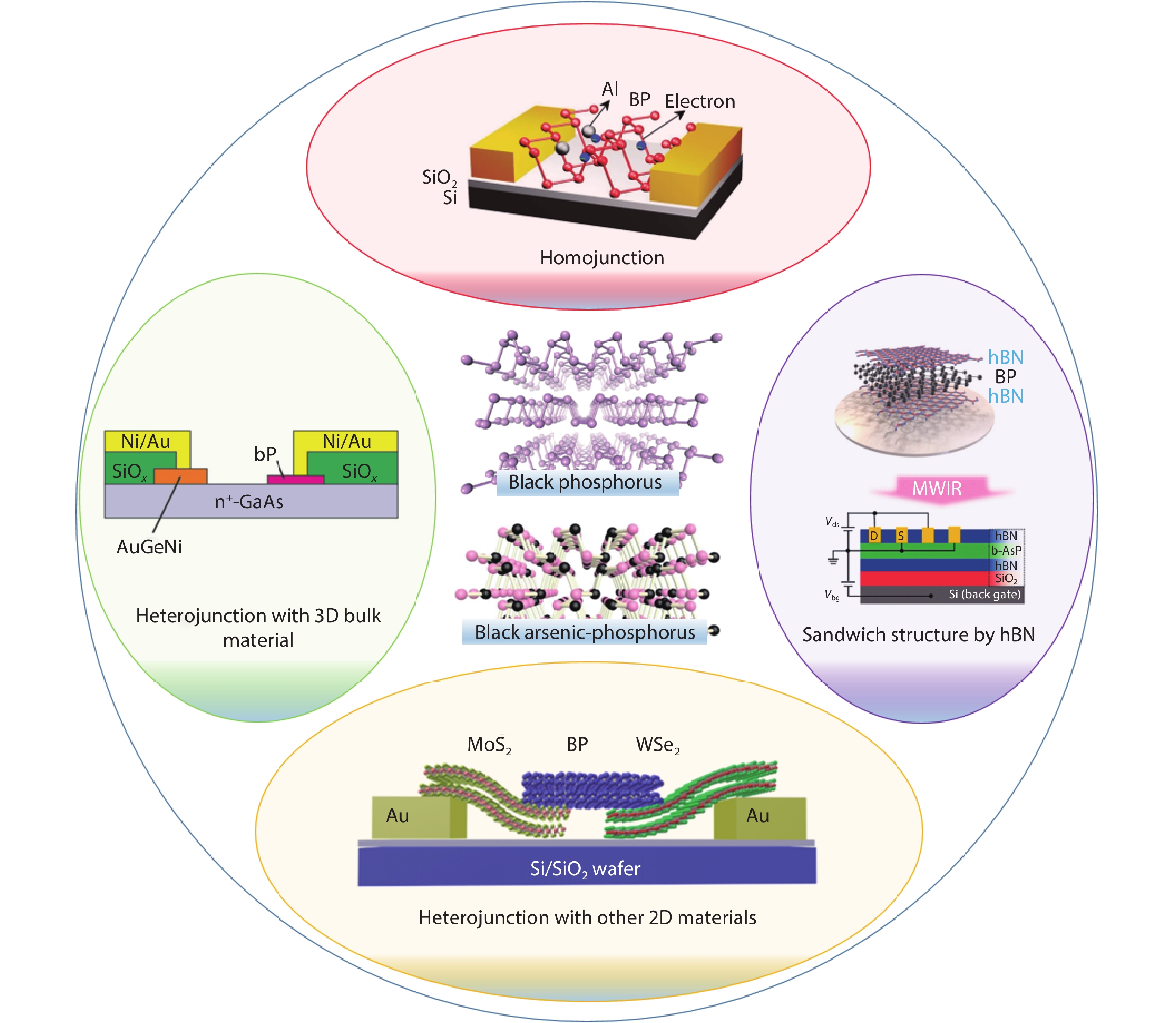
    In this review, as shown in Fig. 1, we will introduce the BP sandwich structure with hBN, BP homojunction devices, BP heterojunction devices with other 2D and 3D bulk materials, and BP doped by As with tunable bandgap. There are three important issues (interface contact, interfacial modification and carrier separation) related to the BP electrical and optoelectronic devices. (1) For BP interface contact, different work-function metals can enable different transport behaviors. If Au or Ni is used, since the work function of Au is close to the middle of the bandgap of BP, so BP FET shows bipolar transport[29]. If high work function metal Pd is used, BP FET shows more like a p-FET[53]. If low work function metal Al is used for BP, n-FET is formed[102]. Typically, there is a Fermi-pining effect between BP and contact, which needs further exploration for contact optimization. (2) BP suffers from stability issues[103]. There is POx forming on both sides of BP[104]. There are several ways to enhance the stability: hBN protection[61], AlOx protection[105], and chemical protection[106]. These methods are very efficient to enhance the stability of the BP film with long time. (3) For BP photodetectors, the carrier separation is the key to enable the photodetection. If the BP is intrinsic, the carrier separation can be speedy, but the photoresponsivity can be relatively low[81]. For intrinsic BP with a perfect lattice structure, the electron–hole pair can be separated easily in BP based on the photovoltaic effect. Youngblood et al. found the largest photocurrent produced under VG = –8 V with a high response bandwidth exceeding 3 GHz, which is related to the intrinsic region of BP under photovoltaic effect [81]. The photo-gating effect cannot dominate in the above case because the trapping center is not enough in high-quality BP. Supposing the BP is doped by E-field or chemical and there is carrier trapping during the separation (i.e. photo-gating effect), in that case, the photoresponsivity can be very high, but the speed can be relatively low. For doped BP with enough trapping centers due to the degradation in air, the photo-gating effect can dominate the photo-sensing behaviors. Guo et al. reported high gain BP photodetectors based on the largest photocurrent produced at the BP doped region, which is related to the doped region of BP under the photo-gating effect[70]. There is a trade-off between choosing high photoresponsivity and response-speed.

    (Color online) Overview of BP crystal structure and BP devices.

    Figure 1.(Color online) Overview of BP crystal structure and BP devices.

    2. Black phosphorus sandwich structure with hBN

    Hexagonal boron nitride is a large-bandgap and chemically stable two-dimensional dielectric material, usually forming a sandwich structure with black phosphorus (Fig. 2(a)). As shown in Fig. 2(b), density functional theory calculation shows that characters such as direct bandgap and linear dichroism are preserved when capping an hBN layer on to protect BP[39]. Cai et al. concludes that hBN is a suitable material for capping BP, protecting it against structural and chemical degradation while still maintaining its major electronic characteristics. The hBN layers’ surface is smoother than SiO2 and is free of dangling bonds and surface charge traps. Thus, hBN is widely used as a substrate to improve the transport properties of other 2D materials[40-44].

    (Color online) Black phosphorus sandwich structure integration with hBN and its band structure. (a) A 3D schematic of hBN/BP/hBN heterostructure. (b) The HSE06 calculation results of the band structure and the local density of states (LDOS) for the hBN/BP heterostructure. Modified with permission from Ref. [38] Copyright 2016 American Chemical Society, (b) Ref. [39] Copyright 2015 American Chemical Society.

    Figure 2.(Color online) Black phosphorus sandwich structure integration with hBN and its band structure. (a) A 3D schematic of hBN/BP/hBN heterostructure. (b) The HSE06 calculation results of the band structure and the local density of states (LDOS) for the hBN/BP heterostructure. Modified with permission from Ref. [38] Copyright 2016 American Chemical Society, (b) Ref. [39] Copyright 2015 American Chemical Society.

    Combining the advantages of hBN, researchers have realized the hBN/BP/hBN structure to improve the transport properties and stability of BP (Fig. 3(a)). Tao et al. calculated the physical properties of hBN/BP/hBN heterostructures with different hBN thicknesses[49]. Compared with monolayer (ML) BP, the bandgap of the hBN(1ML)/BP(ML)/hBN(1ML) trilayer structure was increased by 0.15 eV. However, when the thickness of hBN continuously increased, the bandgap of BP had little change. They also observed an increased hole and electron effective masses via increasing hBN thickness. Doganov et al. compared mobilities of different substrate dielectrics of BP-based FET as a function of temperature, including BP/SiO2, BP/hBN, and hBN/BP/hBN. These results show that the hBN substrate improves mobility compared with SiO2 due to the higher dielectric constant. Furthermore, the full encapsulation with hBN increased the mobility over 100 cm2/(V·s) as shown in Fig. 3(b)[45]. Geim et al. assembled hBN/BP/hBN heterostructure using the dry transfer method in an inert atmosphere. They used monolayer or bilayer hBN on top of BP to protect it from all gases and liquids, and the top hBN layer can let electrons tunnel through, so the electrical contacts can be evaporated onto it without etching openings in the encapsulation. They achieved field-effect mobility of over 4000 cm2/(V·s) for bulklike devices (>10 layers) and about 1200 cm2/(V·s) in a trilayer device (Fig. 3(c)). Moreover, it also showed long-term stability according to the experimental electrical results stored in the air. Quantum oscillations were observed in hBN/BP/hBN sandwiched structures[46]. Nathaniel et al. fabricated the structure with one-dimensional edge contact to metal electrodes. As temperature decreased, the transistor behaved as a gate-dependent metal–insulator transition and device mobility increased. At T = 1.5 K, the mobility reached as high as 4000 cm2/(V·s). Under the condition of moderate magnetic fields and low temperature, they observed gate-tunable Shubnikov de Haas (SdH) magneto-oscillations and Zeeman splitting with an estimated g-factor ~2[32]. Xiaolong et al. used a high-temperature annealing process to reduce the charge trap density in BP. They realized high field-effect mobility of 1350 cm2/(V·s) at room temperature and higher mobility of 2700 cm2/(V·s) at T = 1.7 K. Meanwhile, they observed quantum oscillations and zero Berry phase at the suitable magnetic field and low temperature[30].

    (Color online) Fabrication process and mobility of hBN/BP/hBN heterostructure devices. (a) A 3D schematic of hBN/BP/hBN heterostructure device fabrication process. (b) Mobility results of the different structures including BP/SiO2 (red), BP/hBN (green), and hBN/BP/hBN (blue). (c) Mobility results of the trilayer and 20-layer were measured at liquid helium temperatures. (d) Mobility as a function of temperature for different carrier densities were measured. (e) Quantum Hall states with filling factors from 2 to 12 are observed. (f) FET and Hall mobilities at different temperature. Modified with permission from (a) Ref. [30] Copyright Nature publishing group, (b) Ref. [45] Copyright AIP Publishing, (c) Ref. [46] Copyright 2015 American Chemical Society, (d) and (e) Ref. [47] Copyright 2016 American Chemical Society, (f) Ref. [48] Copyright 2018 American Chemical Society.

    Figure 3.(Color online) Fabrication process and mobility of hBN/BP/hBN heterostructure devices. (a) A 3D schematic of hBN/BP/hBN heterostructure device fabrication process. (b) Mobility results of the different structures including BP/SiO2 (red), BP/hBN (green), and hBN/BP/hBN (blue). (c) Mobility results of the trilayer and 20-layer were measured at liquid helium temperatures. (d) Mobility as a function of temperature for different carrier densities were measured. (e) Quantum Hall states with filling factors from 2 to 12 are observed. (f) FET and Hall mobilities at different temperature. Modified with permission from (a) Ref. [30] Copyright Nature publishing group, (b) Ref. [45] Copyright AIP Publishing, (c) Ref. [46] Copyright 2015 American Chemical Society, (d) and (e) Ref. [47] Copyright 2016 American Chemical Society, (f) Ref. [48] Copyright 2018 American Chemical Society.

    Quantum Hall (QH) effect was observed in hBN/BP/hBN two-dimensional electron systems (2DES). Likai et al. improved mobility of the system by placing the hBN-encapsulated BP on a graphite back gate. The graphite gate results in a high carrier Hall mobility up to 6000 cm2/(V·s) at temperatures T < 30 K. The high mobility enabled them to observe the integer QH effect in BP. QH plateaus were observed at integer filling factors ν from 1 to 7[50]. Long et al. measured hole mobility of the hBN/BP/hBN field-effect transistor on SiO2/Si substrate. The mobility was 5200 cm2/(V·s) at room temperature, and increased to 45 000 cm2/(V·s) at cryogenic temperatures (Fig. 3(d)). They observed QH plateaus at ν from 2 to 12 (Fig. 3(e))[47]. Chen et al. reported a systematic study for thin-layer BP-based hBN/BP/hBN structure. They achieved the high intrinsic saturation velocity of holes and electrons at room temperature. As shown in Fig. 3(f), the FET and Hall mobilities can reach up to 3388 and 2024 cm2/(V·s), respectively[48]. In order to compare the transport properties of black phosphorus BP and BP heterostructures, we list mobilities and on/off ratio for various BP and BP-related heterostructures at different experimental temperatures in Table 1. Most of the BP devices show mobility less than 1000 cm2/(V·s), while the hBN/BP/hBN sandwich structures show the improved mobility larger than 1000 cm2/(V·s). There is strong evidence that the hBN/BP/hBN can enhance the mobility.

    Table Infomation Is Not Enable

    3. Black phosphorus homojunction by dual-gate structure

    The p–n junction is a fundamental building block for the realization of incumbent electronic and optoelectronic devices. In conventional semiconductors, substitutional doping is commonly used to gain n- or p-type characteristics. BP, an ambipolar 2D material, can form n–n, n–p, p–n, and p–p junctions by doping or combining with other 2D materials such as hBN or graphene, respectively. Buscema et al. fabricated p–n junctions based on 2D materials, namely, hBN and BP, which are gate dielectric and channel material, respectively. They observed photovoltaic properties and the detection wavelength up to the near-infrared. Meanwhile, the transfer curves can be turned into four operational quadrants by different gate voltages (Fig. 4)[65]. Liu et al. reported a controllable doping technique using Al atoms to realize a high-performance photovoltaic device, which enhanced 2.5 times electron mobility. The open-circuit voltage responsivity and a short-circuit current responsivity reached ~15.7 × 10³ V/W and ~6.2 mA/W at room temperature in the near-infrared (1550 nm), respectively[60]. Han et al. demonstrated that the electron mobility of BP could be increased one order of magnitude through in situ functionalization of potassium[59]. Recently, Tian et al. reported 2D junctions made of BP and graphene whose type of device can be controlled by the back gate and graphene gate[66]. BP is regarded as a promising material for high speed, high response, and comprehensive spectrum detection from visible to mid-IR at room temperature.

    (Color online) Drain current mapping and band diagrams of the few-layer black phosphorus PN junction. Drain current mapping at (a) + 100 mV and (b) –100 mV as a function of Vrg and VIg, respectively. (c) Schematic energy band diagrams of the different device configurations. Modified with permission from Ref. [65] Copyright 2014 Springer Nature.

    Figure 4.(Color online) Drain current mapping and band diagrams of the few-layer black phosphorus PN junction. Drain current mapping at (a) + 100 mV and (b) –100 mV as a function of Vrg and VIg, respectively. (c) Schematic energy band diagrams of the different device configurations. Modified with permission from Ref. [65] Copyright 2014 Springer Nature.

    4. Black phosphorus heterojunction with other 2D materials (graphene, MoS2, etc.)

    In the conventional p–n homojunction, the p- and n-type regions are formed by chemically doping a bulk semiconductor depleted of free charge carriers, creating built-in potentials. However, 2D semiconductors like BP, graphene, and transition metal dichalcogenides (TMDCs) can stack, forming their unique van der Waals (vdW) structures, which are predicted to exhibit utterly different charge transport characteristics than bulk heterojunctions. The novel bulk crystals are composed of individual layers, in which the van der Waals forces vertically stack each layer instead of covalent bonds. Because of their particular structures, they have great potential for the next-generation electronic and optoelectronic applications[77-79]. BP could stack with other 2D materials to form heterojunctions that reveal unusual properties and new phenomena.

    4.1. Graphene and black phosphorus

    Two-dimensional materials such as graphene have exhibited excellent optical characteristics and offer an attractive prospect for next-generation optoelectronics applications. Graphene has been used for the wideband photodetection from ultraviolet to terahertz[80]. However, graphene photodetectors' dark current is very high due to the graphene lack of a bandgap. Youngblood et al. fabricated a gated multilayer black phosphorus photodetector. The device's dark current is only 220 nA (VG = −8 V, Vbias = −0.4 V). Moreover, the intrinsic responsivity can reach up to 135 and 657 mA/W in 11.5-nm- and 100-nm-thick devices at room temperature, respectively. In almost all aspects of their performance, BP photodetectors are superior to graphene photodetectors[81]. Hu et al. fabricated a 2D hybrid phosphorene and graphene nanocomposite (Fig. 5(a)) and calculated the electronic bandgap using HSE06 method (Fig. 5(b)). The results show that the Fermi velocity of graphene at the Dirac point is kept and open a small bandgap (58 meV), which shows field-effect transistors' potential graphene/BP heterojunction[82]. Avsar et al. realized vertical field-effect transistors (VFETs) based on graphene/BP van der Waals heterostructure, which achieved an on/off ratio of ~100 at room temperature (Fig. 5(c))[61]. Kang et al. realized an on/off ratio of over 800 at 30 K and high on-state current densities of over 1600 A/cm2 in graphene/BP VFETs (Fig. 5(d))[64]. Besides, BP/graphene composite has a widely attracted ion battery research field due to the highest theoretical capacity of phosphorus, high electronic conductivity, mechanical strength, and fast reaction kinetics of graphene[83-86].

    (Color online) Bandgap and structure of graphene/BP heterojunction. (a) The top and side views of schematics of BP (violet)/graphene (gray) heterojunction. (b) The HSE06 calculation results of the band structure are graphene, phosphorene and graphene/BP heterojunction, respectively. (c) Transfer characteristic curves for an encapsulated device by measuring under both vacuum and ambient conditions. The inset shows a nonencapsulated device test. (d) Transfer characteristic curves at ranging various temperatures from 300 to 30 K in 30 K steps. Modified with permission from (a) and (b) Ref. [82] Copyright Royal Society of Chemistry, (c) Ref. [61] Copyright 2015 American Chemical Society, (d) Ref. [64] Copyright 2016 American Chemical Society.

    Figure 5.(Color online) Bandgap and structure of graphene/BP heterojunction. (a) The top and side views of schematics of BP (violet)/graphene (gray) heterojunction. (b) The HSE06 calculation results of the band structure are graphene, phosphorene and graphene/BP heterojunction, respectively. (c) Transfer characteristic curves for an encapsulated device by measuring under both vacuum and ambient conditions. The inset shows a nonencapsulated device test. (d) Transfer characteristic curves at ranging various temperatures from 300 to 30 K in 30 K steps. Modified with permission from (a) and (b) Ref. [82] Copyright Royal Society of Chemistry, (c) Ref. [61] Copyright 2015 American Chemical Society, (d) Ref. [64] Copyright 2016 American Chemical Society.

    4.2. TMDCs and black phosphorus

    TMDCs are atomically thin two-dimensional semiconductors of the type MX2. M is a transition metal atom (Mo, Re, etc.) and X is a chalcogen atom (S, Se, etc.). Molybdenum disulfide (MoS2) is the most exciting material in the TMDCs owing to its robustness[87]. MoS2 has been reported in the research of photodetectors due to unique optoelectronic properties[88-90]. BP-based optoelectronic devices are also widely researched, especially in the advantages of the near-infrared and infrared bands due to the lattice structure and band structure of BP[67-71]. Deng et al. designed a gate-tunable p–n diode based on a p-type BP/n-type monolayer MoS2 van der Waals p–n heterojunction which is the first 2D heterostructure demonstrated using black phosphorus. In the experiments, monolayer MoS2 was synthesized by chemical vapor deposition (CVD) on 285 nm SiO2/p+-doped Si substrate, and the BP was mechanically exfoliated on the monolayer MoS2. The thicknesses of the few-layer BP flake and monolayer MoS2 are 11 and 0.9 nm, respectively. The diodes based on 2D materials achieved a maximum photodetection responsivity of 418 mA/W and photovoltaic energy generation with an external quantum efficiency of 0.3% under the illumination of 633 nm He–Ne laser[72]. Taking advantage of BP bandgap in the infrared, Ye et al. fabricated a diode based on BP/MoS2 heterojunction as shown in Fig. 6(a). It realized microsecond response speed ~15 μs, which is 2 to 3 orders higher than that of the BP-based non-heterojunction photodetector in the near-infrared (Fig. 6(b))[74]. Kwak et al. performed a BP/WS2 heterojunction device at 405 nm and solar spectrum. The external quantum efficiency and the photovoltaic efficiencies are 4.4% and 4.6%, respectively, which shows potential for photovoltaic applications[91]. In addition to combining two materials, the structure's heterojunction has also been reported. Li et al. realized a bipolar phototransistor based on WSe2/BP/MoS2 heterostructure (Fig. 6(c)). As shown in Fig. 6(d), a broadband detector has a high responsivity of 6.32 A/W at visible light and 1.12 A/W at the infrared light, respectively[75]. The value of the photoresponsivity is an order of magnitude higher than that of the detector based on the WSe2/BP heterostructure. Besides, Srivastava et al. fabricated a BP/rhenium disulfide (ReS2) broken-gap van der Waals heterojunction device as shown in Fig. 6(e). Its photoresponsivity and the maximum external quantum efficiency (EQE) can reach up to 8 mA/W (Fig. 6(f)) and 0.3% under illustration under the illumination of 532 nm laser[76].

    (Color online) The photodetectors based on TMDCs/BP heterojunctions. (a) A 3D schematic of the BP/MoS2 heterojunction device. (b) On/off switching characteristics of the BP/MoS2 junction device under illumination of 1.55 μm laser (Laser power 96.2 μW) at different bias voltages. The rise time and the decay were 15 μs and 70 μs, respectively. (c) A 3D schematic of the WSe2/BP/MoS2 heterojunction device. (d) Photoresponsivity and photogain of the WSe2/BP/MoS2 heterojunction device as a function of wavelength, respectively. (e) A 3D schematic diagram of the ReS2/BP heterojunction device. (f) Current rectifying output characteristics as a function of incident laser power values under illumination of 532 nm laser. Modified with permission from (a) and (b) Ref. [74] Copyright 2016 American Chemical Society, (c) and (d) Ref. [75] Copyright 2017 American Chemical Society, (e) and (f) Ref. [76] Copyright 2019 American Chemical Society.

    Figure 6.(Color online) The photodetectors based on TMDCs/BP heterojunctions. (a) A 3D schematic of the BP/MoS2 heterojunction device. (b) On/off switching characteristics of the BP/MoS2 junction device under illumination of 1.55 μm laser (Laser power 96.2 μW) at different bias voltages. The rise time and the decay were 15 μs and 70 μs, respectively. (c) A 3D schematic of the WSe2/BP/MoS2 heterojunction device. (d) Photoresponsivity and photogain of the WSe2/BP/MoS2 heterojunction device as a function of wavelength, respectively. (e) A 3D schematic diagram of the ReS2/BP heterojunction device. (f) Current rectifying output characteristics as a function of incident laser power values under illumination of 532 nm laser. Modified with permission from (a) and (b) Ref. [74] Copyright 2016 American Chemical Society, (c) and (d) Ref. [75] Copyright 2017 American Chemical Society, (e) and (f) Ref. [76] Copyright 2019 American Chemical Society.

    Depending on the carrier transport path, the FET structure based on vdW heterostructures is mainly divided into two categories: lateral heterojunction structure and vertical heterojunction structure. In a lateral heterojunction, the "edge-to-edge" structure allows carriers to conduct primaries in the material plane. However, the "up–down" structure allows carriers to conduct primarily between layers of material for a vertical heterojunction. Xu et al. fabricated a tunneling field-effect transistor based on a BP/MoS2 junction. The device's subthreshold swing (SS) values were ~65 and 51 mV/dec at room temperature and 160 K, respectively[62]. For vertical heterojunctions, they are mainly used for vertical field-effect transistors. This type of device's implementation is mainly due to the excellent quality interlayer conductivity of the two-dimensional semiconductor material. Liu et al. realized a BP/MoS2 tunneling heterojunction diode (Fig. 7(a)). They observed three kinds of diode characteristics, including a backward rectifying diode, a Zener diode, and a forward rectifying diode tuned by the thickness of BP (Fig. 7(b))[63]. Miao et al. realized a truly vertical p–n heterojunction diode based on MoS2/BP heterojunction (Fig. 7(c)). The p–n junction of the vertical structure exhibits a higher on current density than that of the lateral p–n junction. Moreover, they used MoS2 to isolate the effects of air increasing device lifetime (Fig. 7(d))[92]. A comparison of photodetectors based on BP and BP heterostructures is listed in Table 2. The BP/MoS2 heterojunction device shows a faster photo-response speed down to 15 μs than BP FETs around 1 ms.

    (Color online) Structure and performance of the lateral and vertical BP/MoS2 heterostructures. (a) A 3D schematic of the BP/MoS2 heterojunction device. (b) The diode current (Id) as a function of the voltage across the diode at different thicknesses of BP which are 9, 36 and 61 nm, respectively. (c) A schematic diagram of the BP/MoS2 heterostructure device cross-section. (d) I–V characteristics of vertical and lateral BP/MoS2 heterojunction diodes. The inset shows semilogarithmic scale plot of the same I–V curves. Modified with permission from (a) and (b) Ref. [63] Copyright 2017 American Chemical Society, (c) and (d) Ref. [92] Copyright 2017 American Chemical Society.

    Figure 7.(Color online) Structure and performance of the lateral and vertical BP/MoS2 heterostructures. (a) A 3D schematic of the BP/MoS2 heterojunction device. (b) The diode current (Id) as a function of the voltage across the diode at different thicknesses of BP which are 9, 36 and 61 nm, respectively. (c) A schematic diagram of the BP/MoS2 heterostructure device cross-section. (d) I–V characteristics of vertical and lateral BP/MoS2 heterojunction diodes. The inset shows semilogarithmic scale plot of the same I–V curves. Modified with permission from (a) and (b) Ref. [63] Copyright 2017 American Chemical Society, (c) and (d) Ref. [92] Copyright 2017 American Chemical Society.

    Table Infomation Is Not Enable

    5. Black phosphorus heterojunction with 3D bulk material

    The 2D material can be combined with 3D bulk material to form a new heterojunction due to their atomic thin body thickness and the lack of dangling bonds on the surfaces. The integration of 2D material with bulk material can also promote industry applications. The mixed-dimensional 2D/3D vdW heterostructures can improve optical absorption cross-sections than all-2D vdW heterostructures[93]. Gehring et al. transferred a thin-layer BP (~15 nm) sheet onto Te-doped GaAs substrate to form a heterojunction. The maximum EQE of the device can reach 9.7% under the illumination of 514 nm laser at zero bias (Fig. 8(a)) and be increased to 31% at a bias of –2.5 V[94]. Besides, 2D–3D p–n heterojunctions can become easily doped and have a high breakdown electric field for field-effect devices. Li et al. reported a vdW heterojunction JFET based on p-type BP and n-type β-Ga2O3. It exhibits excellent rectification characteristics and low reverse current in the order of picoamperes. Moreover, the source–drain current switching ratio can reach 107 (Fig. 8(b))[96]. Bi et al. realized two kinds of structures: tunnel field-effect transistor (TFET) and junction field-effect transistor (JFET) via the integration of InGaZnO and BP. The TFET’s current switching ratio achieved over 105, and the device's SS values was about 11 mV/dec. Meanwhile in BP/InGaZnO heterostructure JFET, it also shows on/off ratio over 105, almost no hysteresis and larger SS of 83 mV/dec due to the limitation of thermal emission (Fig. 8(c))[109].

    (Color online) Performance of BP/ 3D bulk material heterojunction device. (a) EQE as a function of laser power for different laser light wavelengths at zero source–drain bias based on BP/GaAs heterojunction. (b) Semi-log plot of the transfer characteristics of the JFET based on BP/β-Ga2O3 heterojunction. (c) The transfer characteristics of BP/InGaZnO JFET. The inset shows the corresponding µFE value. Modified with permission from (a) Ref. [94] Copyright AIP publishing, (b) Ref. [96] Copyright 2020 IOP, (c) Ref. [109] Copyright 2020 John Wiley and Sons.

    Figure 8.(Color online) Performance of BP/ 3D bulk material heterojunction device. (a) EQE as a function of laser power for different laser light wavelengths at zero source–drain bias based on BP/GaAs heterojunction. (b) Semi-log plot of the transfer characteristics of the JFET based on BP/β-Ga2O3 heterojunction. (c) The transfer characteristics of BP/InGaZnO JFET. The inset shows the corresponding µFE value. Modified with permission from (a) Ref. [94] Copyright AIP publishing, (b) Ref. [96] Copyright 2020 IOP, (c) Ref. [109] Copyright 2020 John Wiley and Sons.

    6. BP doped by As with tunable bandgap

    Black phosphorus doped by arsenic or black arsenic–phosphorus (b-AsP), a family of layered semiconductors, has attracted extensive attention due to the excellent tunability of bandgaps. Liu et al. demonstrated the bandgap could be tuned to 0.15 eV smaller than BP (0.3 eV). It means that the detection range of the photodetectors based on b-AsP can reach the long-wavelength infrared (LWIR) (Figs. 9(a) and 9(b))[95]. Long et al. fabricated long-wavelength IR, the detection range up to 8.2 μm, photodetectors based on b-AsP. They achieved fast photoresponse (0.54 ms) tested in the mid-wavelength infrared, as shown in Fig. 9(c). Furthermore, this type of device had low dark noise at room temperature whose peak specific detectivity value can reach up to 9.2 × 10⁹ Jones (Fig. 9(d))[97]. B-AsP can also be combined with hBN to form a sandwich structure the same as BP. Yuan et al. fabricated a photodetector based on hBN/b-As0.83P0.17/hBN structure, which achieved good responsivity in the mid-infrared. Moreover, the air stability of the type of device enhanced owing to the hBN encapsulation[98].

    (Color online) Performance of the related b-AsP photodetectors. (a) Infrared absorption as a function of wavenumber for different samples including b-P, b-As0.25P0.75, b-As0.4P0.6 and b-As0.83P0.17, respectively. (b) Bandgap and wavelength as a function of different composition-tunable b-AsxP1−x or different polarization angle of the same composition, respectively. (c) Response curve as a function of time under illumination of 4.034 μm of the b-AsP photodetector. (d) Specific detectivity of different detectors as a function of wavelength including a thermistor bolometer, a PbSe detector, a b-AsP FET device and a b-AsP/MoS2 heterostructure. Modified with permission from (a) and (b) Ref. [95] Copyright John Wiley and Sons, (c) and (d) Ref. [97] Copyright AAAS.

    Figure 9.(Color online) Performance of the related b-AsP photodetectors. (a) Infrared absorption as a function of wavenumber for different samples including b-P, b-As0.25P0.75, b-As0.4P0.6 and b-As0.83P0.17, respectively. (b) Bandgap and wavelength as a function of different composition-tunable b-AsxP1−x or different polarization angle of the same composition, respectively. (c) Response curve as a function of time under illumination of 4.034 μm of the b-AsP photodetector. (d) Specific detectivity of different detectors as a function of wavelength including a thermistor bolometer, a PbSe detector, a b-AsP FET device and a b-AsP/MoS2 heterostructure. Modified with permission from (a) and (b) Ref. [95] Copyright John Wiley and Sons, (c) and (d) Ref. [97] Copyright AAAS.

    7. Summary and perspectives

    In this review, heterostructures based on BP and their electrical and optical applications were discussed in detail. With the tremendous development of applications based on BP owing to its superior characteristics, an increasing number of novel devices based on BP broadly potential from laboratory research to practical use. To achieve this goal, researchers have to suffer from several challenging problems in further research and some possible solutions for dealing with the challenges as follows. (1) Synthesize high-quality wafer-scale crystalline and controllable thicknesses of BP. Fabrication of controllable thicknesses of BP with high quality is essential to design the BP-based devices and applications due to the thickness-dependent intrinsic direct bandgap. Most recently, Xu et al. show the large-area of BP grown on insulating silicon substrates by a gas-phase growth method[107]. It is promising to use the gas-phase growth method for wafer-scale BP. Until now, wafer-scale BP films have not been produced, which greatly hinder the BP-based large-scale applications. (2) Enhancement of long-term stability for BP-based device. Although many strategies have been attempted to improve BP devices' long-term stability, including functionalization, doping, and passivation, the experimental results still show a long distance with commercial grade products. To enhance the long-term stability for BP-based devices for commercial-grade products, a vacuum package can be considered. (3) The BP-based integrated circuits. The complementary inverter is the fundamental building block for logic circuits. Some BP-based complementary inverters have been fabricated via the adatom doping technique[68, 99, 100] or BP hybrids[101]. The uniformity of BP devices is still required to enable large-scale integrated circuits. The MoS2 1-bit microprocessor has been done[108]. The BP-based integrated circuits should come true soon, right after obtaining the wafer-scale BP film. If the large-scale BP can be obtained, there is also a great potential to enable an array of BP photodetectors for middle-IR photo-detection at room temperature, which could be better than the commercial HgCdTe middle-IR photo-detectors. Moreover, the high mobility and reasonable on/off ratio of the BP FET can enable next-generation flexible electronics and circuits with high performance, which is better than the organic-based flexible electronics.

    Acknowledgements

    This work was supported in part by Fundamental Research Project of National Institute of Metrology China under Grant AKYZZ2116, in part by National Natural Science Foundation of China under Grant 62022047, Grant 61874065 and Grant 51861145202, in part by the National Key R&D Program under Grant 2016YFA0200400, in part by the Research Fund from Beijing Innovation Center for Future Chip and the Independent Research Program of Tsinghua University under Grant 20193080047, in part by Young Elite Scientists Sponsorship Program by CAST under Grant 2018QNRC001, and in part by Fok Ying-Tong Education Foundation under Grant 171051.

    References

    [1] R Van Noorden. Moving towards a graphene world. Nature, 442, 228(2006).

    [2] P Sutter. Epitaxial graphene: How silicon leaves the scene. Nat Mater, 8, 171(2009).

    [3] M M Waldrop. The chips are down for moore's law. Nat News, 530, 144(2016).

    [4] A K Geim, K S Novoselov. The rise of graphene. Nat Mater, 6, 183(2007).

    [5] K I Bolotin, K J Sikes, Z Jiang et al. Ultrahigh electron mobility in suspended graphene. Solid State Commun, 146, 351(2008).

    [6] A A Balandin, S Ghosh, W Bao et al. Superior thermal conductivity of single-layer graphene. Nano Lett, 8, 902(2008).

    [7] S Bae, H Kim, Y Lee et al. Roll-to-roll production of 30-inch graphene films for transparent electrodes. Nat Nanotechnol, 5, 574(2010).

    [8] C Lee, X Wei, J W Kysar et al. Measurement of the elastic properties and intrinsic strength of monolayer graphene. Science, 321, 385(2008).

    [9] F Schwierz. Graphene transistors. Nat Nanotechnol, 5, 487(2010).

    [10] R Sordan, F Traversi, V Russo. Logic gates with a single graphene transistor. Appl Phys Lett, 94, 073305(2009).

    [11] T Deng, Z Zhang, Y Liu et al. Three-dimensional graphene field-effect transistors as high-performance photodetectors. Nano Lett, 19, 1494(2019).

    [12] Y Fang, B Luo, Y Jia et al. Renewing functionalized graphene as electrodes for high-performance supercapacitors. Adv Mater, 24, 6348(2012).

    [13] H Wang, Y Yang, Y Liang et al. Graphene-wrapped sulfur particles as a rechargeable lithium-sulfur battery cathode material with high capacity and cycling stability. Nano Lett, 11, 2644(2011).

    [14] X Miao, S Tongay, M K Petterson et al. High efficiency graphene solar cells by chemical doping. Nano Lett, 12, 2745(2012).

    [15] H Tian, T L Ren, D Xie et al. Graphene-on-paper sound source devices. ACS Nano, 5, 4878(2011).

    [16] H Tian, D Xie, Y Yang et al. Single-layer graphene sound-emitting devices: Experiments and modeling. Nanoscale, 4, 2272(2012).

    [17] G Zhang, H Zhang. Thermal conduction and rectification in few-layer graphene y junctions. Nanoscale, 3, 4604(2011).

    [18] Y Lin, T V Williams, J W Connell. Soluble, exfoliated hexagonal boron nitride nanosheets. J Phys Chem Lett, 1, 277(2009).

    [19] S Balendhran, S Walia, H Nili et al. Elemental analogues of graphene: Silicene, germanene, stanene, and phosphorene. Small, 11, 640(2015).

    [20] Q H Wang, K Kalantar-Zadeh, A Kis et al. Electronics and optoelectronics of two-dimensional transition metal dichalcogenides. Nat Nanotechnol, 7, 699(2012).

    [21] W Wu, D De, S C Chang et al. High mobility and high on/off ratio field-effect transistors based on chemical vapor deposited single-crystal MoS2 grains. Appl Phys Lett, 102, 142106(2013).

    [22] A Carvalho, M Wang, X Zhu et al. Phosphorene: From theory to applications. Nat Rev Mater, 1, 1(2016).

    [23] P W Bridgman. Two new modifications of phosphorus. J Am Chem Soc, 36, 1344(1914).

    [24] H Liu, A T Neal, Z Zhu et al. Phosphorene: An unexplored 2D semiconductor with a high hole mobility. Acs Nano, 8, 4033(2014).

    [25] A Castellanos-Gomez, L Vicarelli, E Prada et al. Isolation and characterization of few-layer black phosphorus. 2D Mater, 1, 025001(2014).

    [26] S P Koenig, R A Doganov, H Schmidt et al. Electric field effect in ultrathin black phosphorus. Appl Phys Lett, 104, 103106(2014).

    [27] V Tran, R Soklaski, Y Liang et al. Layer-controlled band gap and anisotropic excitons in few-layer black phosphorus. Phys Rev B, 89, 235319(2014).

    [28] M Engel, M Steiner, P Avouris. Black phosphorus photodetector for multispectral, high-resolution imaging. Nano Lett, 14, 6414(2014).

    [29] L Li, Y Yu, G J Ye et al. Black phosphorus field-effect transistors. Nat Nanotechnol, 9, 372(2014).

    [30] X Chen, Y Wu, Z Wu et al. High-quality sandwiched black phosphorus heterostructure and its quantum oscillations. Nat Commun, 6, 7315(2015).

    [31] L Li, G J Ye, V Tran et al. Quantum oscillations in a two-dimensional electron gas in black phosphorus thin films. Nat Nanotechnol, 10, 608(2015).

    [32] N Gillgren, D Wickramaratne, Y Shi et al. Gate tunable quantum oscillations in air-stable and high mobility few-layer phosphorene heterostructures. 2D Mater, 2, 011001(2014).

    [33] R Fei, A Faghaninia, R Soklaski et al. Enhanced thermoelectric efficiency via orthogonal electrical and thermal conductances in phosphorene. Nano Lett, 14, 6393(2014).

    [34] S Lee, F Yang, J Suh et al. Anisotropic in-plane thermal conductivity of black phosphorus nanoribbons at temperatures higher than 100 K. Nat Commun, 6, 8573(2015).

    [35] Z Luo, J Maassen, Y Deng et al. Anisotropic in-plane thermal conductivity observed in few-layer black phosphorus. Nat Commun, 6, 8572(2015).

    [36] Y Saito, T Iizuka, T Koretsune et al. Gate-tuned thermoelectric power in black phosphorus. Nano Lett, 16, 4819(2016).

    [37] J W Jiang, H S Park. Negative poisson’s ratio in single-layer black phosphorus. Nat Commun, 5, 4727(2014).

    [38] G C Constantinescu, N D M Hine. Multipurpose black-phosphorus/hBN heterostructures. Nano Lett, 16, 2586(2016).

    [39] Y Cai, G Zhang, Y W Zhang. Electronic properties of phosphorene/graphene and phosphorene/hexagonal boron nitride heterostructures. J Phys Chem C, 119, 13929(2015).

    [40] C R Dean, A F Young, I Meric et al. Boron nitride substrates for high-quality graphene electronics. Nat Nanotechnol, 5, 722(2010).

    [41] M Y Chan, K Komatsu, S L Li et al. Suppression of thermally activated carrier transport in atomically thin MoS2 on crystalline hexagonal boron nitride substrates. Nanoscale, 5, 9572(2013).

    [42] G H Lee, Y J Yu, X Cui et al. Flexible and transparent MoS2 field-effect transistors on hexagonal boron nitride-graphene heterostructures. ACS Nano, 7, 7931(2013).

    [43] J Xue, J Sanchez-Yamagishi, D Bulmash et al. Scanning tunnelling microscopy and spectroscopy of ultra-flat graphene on hexagonal boron nitride. Nat Mater, 10, 282(2011).

    [44] C Lee, S Rathi, M A Khan et al. Comparison of trapped charges and hysteresis behavior in hBN encapsulated single MoS2 flake based field effect transistors on SiO2 and hBN substrates. Nanotechnology, 29, 335202(2018).

    [45] R A Doganov, S P Koenig, Y Yeo et al. Transport properties of ultrathin black phosphorus on hexagonal boron nitride. Appl Phys Lett, 106, 083505(2015).

    [46] Y Cao, A Mishchenko, G L Yu et al. Quality heterostructures from two-dimensional crystals unstable in air by their assembly in inert atmosphere. Nano Lett, 15, 4914(2015).

    [47] G Long, D Maryenko, J Shen et al. Achieving ultrahigh carrier mobility in two-dimensional hole gas of black phosphorus. Nano Lett, 16, 7768(2016).

    [48] X Chen, C Chen, A Levi et al. Large-velocity saturation in thin-film black phosphorus transistors. ACS Nano, 12, 5003(2018).

    [49] T Hu, J Hong. Anisotropic effective mass, optical property, and enhanced band gap in hBN /phosphorene/ hBN heterostructures. ACS Appl Mater Interfaces, 7, 23489(2015).

    [50] L Li, F Yang, G J Ye et al. Quantum hall effect in black phosphorus two-dimensional electron system. Nat Nanotechnol, 11, 593(2016).

    [51] S Das, M Demarteau, A Roelofs. Ambipolar phosphorene field effect transistor. ACS Nano, 8, 11730(2014).

    [52] F Xia, H Wang, Y Jia. Rediscovering black phosphorus as an anisotropic layered material for optoelectronics and electronics. Nat Commun, 5, 4458(2014).

    [53] Y Du, H Liu, Y Deng et al. Device perspective for black phosphorus field-effect transistors: Contact resistance, ambipolar behavior, and scaling. ACS Nano, 8, 10035(2014).

    [54] H Wang, X Wang, F Xia et al. Black phosphorus radio-frequency transistors. Nano Lett, 14, 6424(2014).

    [55] W Zhu, M N Yogeesh, S Yang et al. Flexible black phosphorus ambipolar transistors, circuits and am demodulator. Nano Lett, 15, 1883(2015).

    [56] M V Kamalakar, B N Madhushankar, A Dankert et al. Low schottky barrier black phosphorus field-effect devices with ferromagnetic tunnel contacts. Small, 11, 2209(2015).

    [57] J Miao, S Zhang, L Cai et al. Ultrashort channel length black phosphorus field-effect transistors. ACS Nano, 9, 9236(2015).

    [58] A Prakash, Y Cai, G Zhang et al. Black phosphorus n-type field-effect transistor with ultrahigh electron mobility via aluminum adatoms doping. Small, 13, 1602909(2017).

    [59] C Han, Z Hu, L C Gomes et al. Surface functionalization of black phosphorus via potassium toward high-performance complementary devices. Nano Lett, 17, 4122(2017).

    [60] Y Liu, Y Cai, G Zhang et al. Al-doped black phosphorus p–n homojunction diode for high performance photovoltaic. Adv Funct Mater, 27, 1604638(2017).

    [61] A Avsar, I J Vera-Marun, J Y Tan et al. Air-stable transport in graphene-contacted, fully encapsulated ultrathin black phosphorus-based field-effect transistors. ACS Nano, 9, 4138(2015).

    [62] J Xu, J Jia, S Lai et al. Tunneling field effect transistor integrated with black phosphorus-MoS2 junction and ion gel dielectric. Appl Phys Lett, 110, 033103(2017).

    [63] X Liu, D Qu, H M Li et al. Modulation of quantum tunneling via a vertical two-dimensional black phosphorus and molybdenum disulfide p–n junction. ACS Nano, 11, 9143(2017).

    [64] J Kang, D Jariwala, C R Ryder et al. Probing out-of-plane charge transport in black phosphorus with graphene-contacted vertical field-effect transistors. Nano Lett, 16, 2580(2016).

    [65] M Buscema, D J Groenendijk, G A Steele et al. Photovoltaic effect in few-layer black phosphorus pn junctions defined by local electrostatic gating. Nat Commun, 5, 4651(2014).

    [66] H Tian, L Li, M A Mohammad et al. High-quality reconfigurable black phosphorus p–n junctions. IEEE Trans Electron Devices, 65, 5118(2018).

    [67] M Buscema, D J Groenendijk, S I Blanter et al. Fast and broadband photoresponse of few-layer black phosphorus field-effect transistors. Nano Lett, 14, 3347(2014).

    [68] J Wu, G K Koon, D Xiang et al. Colossal ultraviolet photoresponsivity of few-layer black phosphorus. ACS Nano, 9, 8070(2015).

    [69] M Huang, M Wang, C Chen et al. Broadband black-phosphorus photodetectors with high responsivity. Adv Mater, 28, 3481(2016).

    [70] Q Guo, A Pospischil, M Bhuiyan et al. Black phosphorus mid-infrared photodetectors with high gain. Nano Lett, 16, 4648(2016).

    [71] C Hou, L Yang, B Li et al. Multilayer black phosphorus near-infrared photodetectors. Sensors, 18, 1668(2018).

    [72] Y Deng, Z Luo, N J Conrad et al. Black phosphorus-monolayer MoS2 van der Waals heterojunction p–n diode. ACS Nano, 8, 8292(2014).

    [73] T Hong, B Chamlagain, T Wang et al. Anisotropic photocurrent response at black phosphorus–MoS2 p–n heterojunctions. Nanoscale, 7, 18537(2015).

    [74] L Ye, H Li, Z Chen et al. Near-infrared photodetector based on MoS2/black phosphorus heterojunction. ACS Photonics, 3, 692(2016).

    [75] H Li, L Ye, J Xu. High-performance broadband floating-base bipolar phototransistor based on WSe2/bp/MoS2 heterostructure. ACS Photonics, 4, 823(2017).

    [76] P K Srivastava, Y Hassan, Y Gebredingle et al. Van der waals broken-gap p–n heterojunction tunnel diode based on black phosphorus and rhenium disulfide. ACS Appl Mater Interfaces, 11, 8266(2019).

    [77] L Huang, N Huo, Y Li et al. Electric-field tunable band offsets in black phosphorus and MoS2 van der Waals p–n heterostructure. J Phys Chem Lett, 6, 2483(2015).

    [78] X Wang, S Lan. Optical properties of black phosphorus. Adv Opt Photonics, 8, 618(2016).

    [79] H Liu, Y Du, Y Deng et al. Semiconducting black phosphorus: Synthesis, transport properties and electronic applications. Chem Soc Rev, 44, 2732(2015).

    [80] H Chen, H Liu, Z Zhang et al. Nanostructured photodetectors: From ultraviolet to terahertz. Adv Mater, 28, 403(2016).

    [81] N Youngblood, C Chen, S J Koester et al. Waveguide-integrated black phosphorus photodetector with high responsivity and low dark current. Nat Photonics, 9, 247(2015).

    [82] W Hu, T Wang, J Yang. Tunable schottky contacts in hybrid graphene–phosphorene nanocomposites. J Mater Chem C, 3, 4756(2015).

    [83] J Song, Z Yu, M L Gordin et al. Chemically bonded phosphorus/graphene hybrid as a high performance anode for sodium-ion batteries. Nano Lett, 14, 6329(2014).

    [84] Z Yu, J Song, M L Gordin et al. Phosphorus-graphene nanosheet hybrids as lithium-ion anode with exceptional high-temperature cycling stability. Adv Sci, 2, 1400020(2015).

    [85] M Li, N Muralidharan, K Moyer et al. Solvent mediated hybrid 2D materials: Black phosphorus – graphene heterostructured building blocks assembled for sodium ion batteries. Nanoscale, 10, 10443(2018).

    [86] Y Liu, Q Liu, A Zhang et al. Room-temperature pressure synthesis of layered black phosphorus-graphene composite for sodium-ion battery anodes. ACS Nano, 12, 8323(2018).

    [87] S Manzeli, D Ovchinnikov, D Pasquier et al. 2D transition metal dichalcogenides. Nat Rev Mater, 2, 17033(2017).

    [88] O Lopez-Sanchez, D Lembke, M Kayci et al. Ultrasensitive photodetectors based on monolayer MoS2. Nat Nanotechnol, 8, 497(2013).

    [89] Z Yin, H Li, H Li et al. Single-layer MoS2 phototransistors. ACS Nano, 6, 74(2012).

    [90] H S Lee, S W Min, Y G Chang et al. MoS2 nanosheet phototransistors with thickness-modulated optical energy gap. Nano Lett, 12, 3695(2012).

    [91] D H Kwak, H S Ra, M H Jeong et al. High-performance photovoltaic effect with electrically balanced charge carriers in black phosphorus and WS2 heterojunction. Adv Mater Interfaces, 5, 1800671(2018).

    [92] J Miao, Z Xu, Q Li et al. Vertically stacked and self-encapsulated van der Waals heterojunction diodes using two-dimensional layered semiconductors. ACS Nano, 11, 10472(2017).

    [93] D Jariwala, T J Marks, M C Hersam. Mixed-dimensional van der Waals heterostructures. Nat Mater, 16, 170(2017).

    [94] P Gehring, R Urcuyo, D L Duong et al. Thin-layer black phosphorus/gaas heterojunction p –n diodes. Appl Phys Lett, 106, 233110(2015).

    [95] B Liu, M Kopf, A N Abbas et al. Black arsenic-phosphorus: Layered anisotropic infrared semiconductors with highly tunable compositions and properties. Adv Mater, 27, 4423(2015).

    [96] C Li, C Chen, J Chen et al. High-performance junction field-effect transistor based on black phosphorus/β-Ga2O3 heterostructure. J Semicond, 41, 082002(2020).

    [97] M Long, A Gao, P Wang et al. Room temperature high-detectivity mid-infrared photodetectors based on black arsenic phosphorus. Sci Adv, 3, e1700589(2017).

    [98] S Yuan, C Shen, B Deng et al. Air-stable room-temperature mid-infrared photodetectors based on hBN/black arsenic phosphorus/ hBN heterostructures. Nano Lett, 18, 3172(2018).

    [99] S P Koenig, R A Doganov, L Seixas et al. Electron doping of ultrathin black phosphorus with Cu adatoms. Nano Lett, 16, 2145(2016).

    [100] L Chen, S Li, X W Feng et al. Gigahertz integrated circuits based on complementary black phosphorus transistors. Adv Electron Mater, 4, 1800274(2018).

    [101] G Gao, B Wan, X Liu et al. Tunable tribotronic dual-gate logic devices based on 2D MoS2 and black phosphorus. Adv Mater, 30, 1705088(2018).

    [102] D J Perello, S H Chae, S Song et al. High-performance n-type black phosphorus transistors with type control via thickness and contact-metal engineering. Nat Commun, 6, 7809(2015).

    [103] A Favron, E Gaufrès, F Fossard et al. Photooxidation and quantum confinement effects in exfoliated black phosphorus. Nat Mater, 14, 826(2015).

    [104] H Tian, Q Guo, Y Xie et al. Anisotropic black phosphorus synaptic device for neuromorphic applications. Adv Mater, 28, 4991(2016).

    [105] J D Wood, S A Wells, D Jariwala et al. Effective passivation of exfoliated black phosphorus transistors against ambient degradation. Nano Lett, 14, 6964(2014).

    [106] C R Ryder, J D Wood, S A Wells et al. Covalent functionalization and passivation of exfoliated black phosphorus via aryl diazonium chemistry. Nat Chem, 8, 597(2016).

    [107] Y Xu, X Shi, Y Zhang et al. Epitaxial nucleation and lateral growth of high-crystalline black phosphorus films on silicon. Nat Commun, 11, 1330(2020).

    [108] S Wachter, D K Polyushkin, O Bethge et al. A microprocessor based on a two-dimensional semiconductor. Nat Commun, 8, 14948(2017).

    [109] J Bi, X Zou, Y Lv et al. Ingazno tunnel and junction transistors based on vertically stacked black phosphorus/ingazno heterojunctions. Adv Electron Mater, 6, 2000291(2020).

    Ningqin Deng, He Tian, Jian Zhang, Jinming Jian, Fan Wu, Yang Shen, Yi Yang, Tian-Ling Ren. Black phosphorus junctions and their electrical and optoelectronic applications[J]. Journal of Semiconductors, 2021, 42(8): 081001
    Download Citation