[1] R Van Noorden. Moving towards a graphene world. Nature, 442, 228(2006).
[2] P Sutter. Epitaxial graphene: How silicon leaves the scene. Nat Mater, 8, 171(2009).
[3] M M Waldrop. The chips are down for moore's law. Nat News, 530, 144(2016).
[4] A K Geim, K S Novoselov. The rise of graphene. Nat Mater, 6, 183(2007).
[5] K I Bolotin, K J Sikes, Z Jiang et al. Ultrahigh electron mobility in suspended graphene. Solid State Commun, 146, 351(2008).
[6] A A Balandin, S Ghosh, W Bao et al. Superior thermal conductivity of single-layer graphene. Nano Lett, 8, 902(2008).
[7] S Bae, H Kim, Y Lee et al. Roll-to-roll production of 30-inch graphene films for transparent electrodes. Nat Nanotechnol, 5, 574(2010).
[8] C Lee, X Wei, J W Kysar et al. Measurement of the elastic properties and intrinsic strength of monolayer graphene. Science, 321, 385(2008).
[9] F Schwierz. Graphene transistors. Nat Nanotechnol, 5, 487(2010).
[10] R Sordan, F Traversi, V Russo. Logic gates with a single graphene transistor. Appl Phys Lett, 94, 073305(2009).
[11] T Deng, Z Zhang, Y Liu et al. Three-dimensional graphene field-effect transistors as high-performance photodetectors. Nano Lett, 19, 1494(2019).
[12] Y Fang, B Luo, Y Jia et al. Renewing functionalized graphene as electrodes for high-performance supercapacitors. Adv Mater, 24, 6348(2012).
[13] H Wang, Y Yang, Y Liang et al. Graphene-wrapped sulfur particles as a rechargeable lithium-sulfur battery cathode material with high capacity and cycling stability. Nano Lett, 11, 2644(2011).
[14] X Miao, S Tongay, M K Petterson et al. High efficiency graphene solar cells by chemical doping. Nano Lett, 12, 2745(2012).
[15] H Tian, T L Ren, D Xie et al. Graphene-on-paper sound source devices. ACS Nano, 5, 4878(2011).
[16] H Tian, D Xie, Y Yang et al. Single-layer graphene sound-emitting devices: Experiments and modeling. Nanoscale, 4, 2272(2012).
[17] G Zhang, H Zhang. Thermal conduction and rectification in few-layer graphene y junctions. Nanoscale, 3, 4604(2011).
[18] Y Lin, T V Williams, J W Connell. Soluble, exfoliated hexagonal boron nitride nanosheets. J Phys Chem Lett, 1, 277(2009).
[19] S Balendhran, S Walia, H Nili et al. Elemental analogues of graphene: Silicene, germanene, stanene, and phosphorene. Small, 11, 640(2015).
[20] Q H Wang, K Kalantar-Zadeh, A Kis et al. Electronics and optoelectronics of two-dimensional transition metal dichalcogenides. Nat Nanotechnol, 7, 699(2012).
[21] W Wu, D De, S C Chang et al. High mobility and high on/off ratio field-effect transistors based on chemical vapor deposited single-crystal MoS2 grains. Appl Phys Lett, 102, 142106(2013).
[22] A Carvalho, M Wang, X Zhu et al. Phosphorene: From theory to applications. Nat Rev Mater, 1, 1(2016).
[23] P W Bridgman. Two new modifications of phosphorus. J Am Chem Soc, 36, 1344(1914).
[24] H Liu, A T Neal, Z Zhu et al. Phosphorene: An unexplored 2D semiconductor with a high hole mobility. Acs Nano, 8, 4033(2014).
[25] A Castellanos-Gomez, L Vicarelli, E Prada et al. Isolation and characterization of few-layer black phosphorus. 2D Mater, 1, 025001(2014).
[26] S P Koenig, R A Doganov, H Schmidt et al. Electric field effect in ultrathin black phosphorus. Appl Phys Lett, 104, 103106(2014).
[27] V Tran, R Soklaski, Y Liang et al. Layer-controlled band gap and anisotropic excitons in few-layer black phosphorus. Phys Rev B, 89, 235319(2014).
[28] M Engel, M Steiner, P Avouris. Black phosphorus photodetector for multispectral, high-resolution imaging. Nano Lett, 14, 6414(2014).
[29] L Li, Y Yu, G J Ye et al. Black phosphorus field-effect transistors. Nat Nanotechnol, 9, 372(2014).
[30] X Chen, Y Wu, Z Wu et al. High-quality sandwiched black phosphorus heterostructure and its quantum oscillations. Nat Commun, 6, 7315(2015).
[31] L Li, G J Ye, V Tran et al. Quantum oscillations in a two-dimensional electron gas in black phosphorus thin films. Nat Nanotechnol, 10, 608(2015).
[32] N Gillgren, D Wickramaratne, Y Shi et al. Gate tunable quantum oscillations in air-stable and high mobility few-layer phosphorene heterostructures. 2D Mater, 2, 011001(2014).
[33] R Fei, A Faghaninia, R Soklaski et al. Enhanced thermoelectric efficiency via orthogonal electrical and thermal conductances in phosphorene. Nano Lett, 14, 6393(2014).
[34] S Lee, F Yang, J Suh et al. Anisotropic in-plane thermal conductivity of black phosphorus nanoribbons at temperatures higher than 100 K. Nat Commun, 6, 8573(2015).
[35] Z Luo, J Maassen, Y Deng et al. Anisotropic in-plane thermal conductivity observed in few-layer black phosphorus. Nat Commun, 6, 8572(2015).
[36] Y Saito, T Iizuka, T Koretsune et al. Gate-tuned thermoelectric power in black phosphorus. Nano Lett, 16, 4819(2016).
[37] J W Jiang, H S Park. Negative poisson’s ratio in single-layer black phosphorus. Nat Commun, 5, 4727(2014).
[38] G C Constantinescu, N D M Hine. Multipurpose black-phosphorus/hBN heterostructures. Nano Lett, 16, 2586(2016).
[39] Y Cai, G Zhang, Y W Zhang. Electronic properties of phosphorene/graphene and phosphorene/hexagonal boron nitride heterostructures. J Phys Chem C, 119, 13929(2015).
[40] C R Dean, A F Young, I Meric et al. Boron nitride substrates for high-quality graphene electronics. Nat Nanotechnol, 5, 722(2010).
[41] M Y Chan, K Komatsu, S L Li et al. Suppression of thermally activated carrier transport in atomically thin MoS2 on crystalline hexagonal boron nitride substrates. Nanoscale, 5, 9572(2013).
[42] G H Lee, Y J Yu, X Cui et al. Flexible and transparent MoS2 field-effect transistors on hexagonal boron nitride-graphene heterostructures. ACS Nano, 7, 7931(2013).
[43] J Xue, J Sanchez-Yamagishi, D Bulmash et al. Scanning tunnelling microscopy and spectroscopy of ultra-flat graphene on hexagonal boron nitride. Nat Mater, 10, 282(2011).
[44] C Lee, S Rathi, M A Khan et al. Comparison of trapped charges and hysteresis behavior in hBN encapsulated single MoS2 flake based field effect transistors on SiO2 and hBN substrates. Nanotechnology, 29, 335202(2018).
[45] R A Doganov, S P Koenig, Y Yeo et al. Transport properties of ultrathin black phosphorus on hexagonal boron nitride. Appl Phys Lett, 106, 083505(2015).
[46] Y Cao, A Mishchenko, G L Yu et al. Quality heterostructures from two-dimensional crystals unstable in air by their assembly in inert atmosphere. Nano Lett, 15, 4914(2015).
[47] G Long, D Maryenko, J Shen et al. Achieving ultrahigh carrier mobility in two-dimensional hole gas of black phosphorus. Nano Lett, 16, 7768(2016).
[48] X Chen, C Chen, A Levi et al. Large-velocity saturation in thin-film black phosphorus transistors. ACS Nano, 12, 5003(2018).
[49] T Hu, J Hong. Anisotropic effective mass, optical property, and enhanced band gap in hBN /phosphorene/ hBN heterostructures. ACS Appl Mater Interfaces, 7, 23489(2015).
[50] L Li, F Yang, G J Ye et al. Quantum hall effect in black phosphorus two-dimensional electron system. Nat Nanotechnol, 11, 593(2016).
[51] S Das, M Demarteau, A Roelofs. Ambipolar phosphorene field effect transistor. ACS Nano, 8, 11730(2014).
[52] F Xia, H Wang, Y Jia. Rediscovering black phosphorus as an anisotropic layered material for optoelectronics and electronics. Nat Commun, 5, 4458(2014).
[53] Y Du, H Liu, Y Deng et al. Device perspective for black phosphorus field-effect transistors: Contact resistance, ambipolar behavior, and scaling. ACS Nano, 8, 10035(2014).
[54] H Wang, X Wang, F Xia et al. Black phosphorus radio-frequency transistors. Nano Lett, 14, 6424(2014).
[55] W Zhu, M N Yogeesh, S Yang et al. Flexible black phosphorus ambipolar transistors, circuits and am demodulator. Nano Lett, 15, 1883(2015).
[56] M V Kamalakar, B N Madhushankar, A Dankert et al. Low schottky barrier black phosphorus field-effect devices with ferromagnetic tunnel contacts. Small, 11, 2209(2015).
[57] J Miao, S Zhang, L Cai et al. Ultrashort channel length black phosphorus field-effect transistors. ACS Nano, 9, 9236(2015).
[58] A Prakash, Y Cai, G Zhang et al. Black phosphorus n-type field-effect transistor with ultrahigh electron mobility via aluminum adatoms doping. Small, 13, 1602909(2017).
[59] C Han, Z Hu, L C Gomes et al. Surface functionalization of black phosphorus via potassium toward high-performance complementary devices. Nano Lett, 17, 4122(2017).
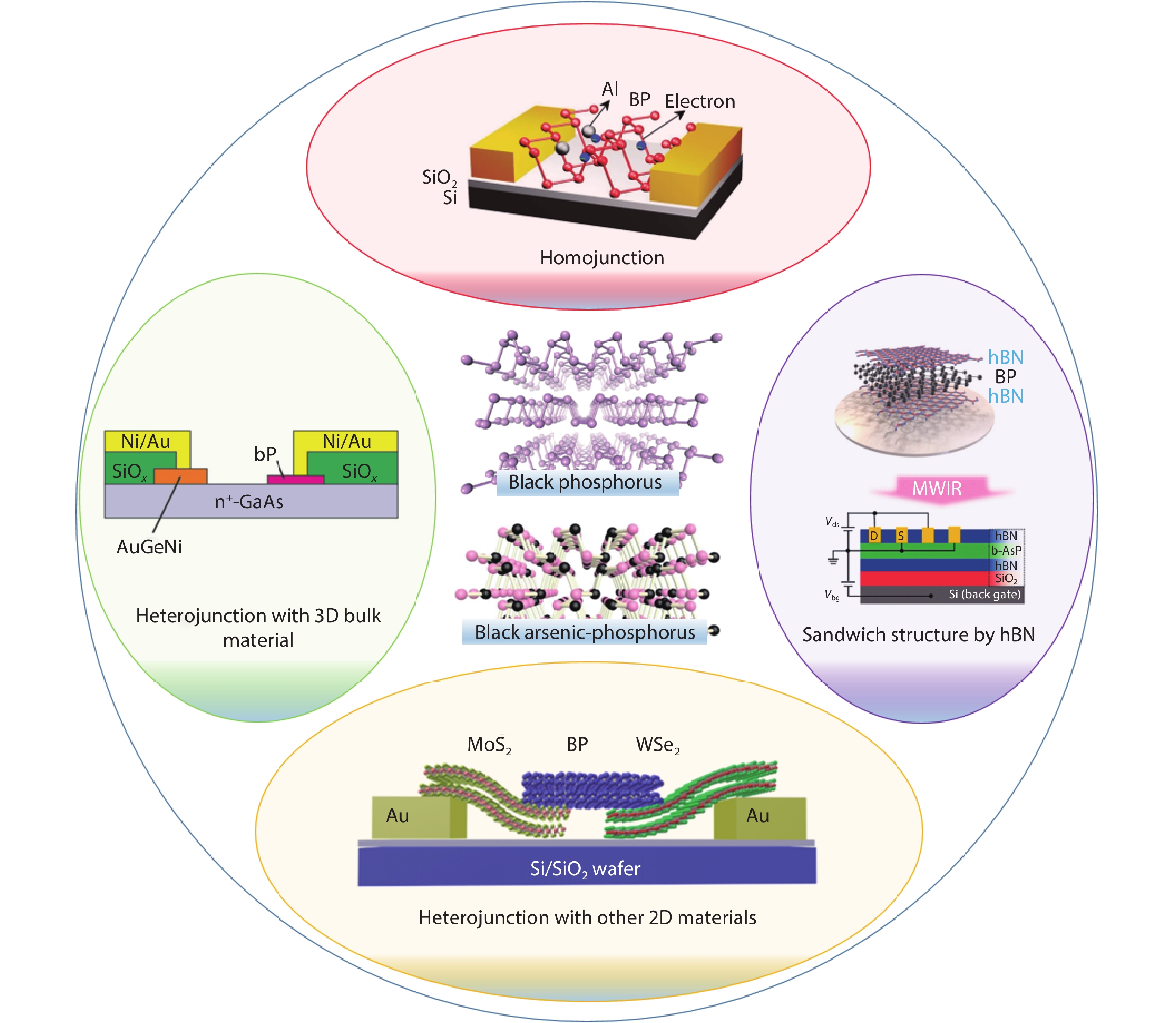
[60] Y Liu, Y Cai, G Zhang et al. Al-doped black phosphorus p–n homojunction diode for high performance photovoltaic. Adv Funct Mater, 27, 1604638(2017).
[61] A Avsar, I J Vera-Marun, J Y Tan et al. Air-stable transport in graphene-contacted, fully encapsulated ultrathin black phosphorus-based field-effect transistors. ACS Nano, 9, 4138(2015).
[62] J Xu, J Jia, S Lai et al. Tunneling field effect transistor integrated with black phosphorus-MoS2 junction and ion gel dielectric. Appl Phys Lett, 110, 033103(2017).
[63] X Liu, D Qu, H M Li et al. Modulation of quantum tunneling via a vertical two-dimensional black phosphorus and molybdenum disulfide p–n junction. ACS Nano, 11, 9143(2017).
[64] J Kang, D Jariwala, C R Ryder et al. Probing out-of-plane charge transport in black phosphorus with graphene-contacted vertical field-effect transistors. Nano Lett, 16, 2580(2016).
[65] M Buscema, D J Groenendijk, G A Steele et al. Photovoltaic effect in few-layer black phosphorus pn junctions defined by local electrostatic gating. Nat Commun, 5, 4651(2014).
[66] H Tian, L Li, M A Mohammad et al. High-quality reconfigurable black phosphorus p–n junctions. IEEE Trans Electron Devices, 65, 5118(2018).
[67] M Buscema, D J Groenendijk, S I Blanter et al. Fast and broadband photoresponse of few-layer black phosphorus field-effect transistors. Nano Lett, 14, 3347(2014).
[68] J Wu, G K Koon, D Xiang et al. Colossal ultraviolet photoresponsivity of few-layer black phosphorus. ACS Nano, 9, 8070(2015).
[69] M Huang, M Wang, C Chen et al. Broadband black-phosphorus photodetectors with high responsivity. Adv Mater, 28, 3481(2016).
[70] Q Guo, A Pospischil, M Bhuiyan et al. Black phosphorus mid-infrared photodetectors with high gain. Nano Lett, 16, 4648(2016).
[71] C Hou, L Yang, B Li et al. Multilayer black phosphorus near-infrared photodetectors. Sensors, 18, 1668(2018).
[72] Y Deng, Z Luo, N J Conrad et al. Black phosphorus-monolayer MoS2 van der Waals heterojunction p–n diode. ACS Nano, 8, 8292(2014).
[73] T Hong, B Chamlagain, T Wang et al. Anisotropic photocurrent response at black phosphorus–MoS2 p–n heterojunctions. Nanoscale, 7, 18537(2015).
[74] L Ye, H Li, Z Chen et al. Near-infrared photodetector based on MoS2/black phosphorus heterojunction. ACS Photonics, 3, 692(2016).
[75] H Li, L Ye, J Xu. High-performance broadband floating-base bipolar phototransistor based on WSe2/bp/MoS2 heterostructure. ACS Photonics, 4, 823(2017).
[76] P K Srivastava, Y Hassan, Y Gebredingle et al. Van der waals broken-gap p–n heterojunction tunnel diode based on black phosphorus and rhenium disulfide. ACS Appl Mater Interfaces, 11, 8266(2019).
[77] L Huang, N Huo, Y Li et al. Electric-field tunable band offsets in black phosphorus and MoS2 van der Waals p–n heterostructure. J Phys Chem Lett, 6, 2483(2015).
[78] X Wang, S Lan. Optical properties of black phosphorus. Adv Opt Photonics, 8, 618(2016).
[79] H Liu, Y Du, Y Deng et al. Semiconducting black phosphorus: Synthesis, transport properties and electronic applications. Chem Soc Rev, 44, 2732(2015).
[80] H Chen, H Liu, Z Zhang et al. Nanostructured photodetectors: From ultraviolet to terahertz. Adv Mater, 28, 403(2016).
[81] N Youngblood, C Chen, S J Koester et al. Waveguide-integrated black phosphorus photodetector with high responsivity and low dark current. Nat Photonics, 9, 247(2015).
[82] W Hu, T Wang, J Yang. Tunable schottky contacts in hybrid graphene–phosphorene nanocomposites. J Mater Chem C, 3, 4756(2015).
[83] J Song, Z Yu, M L Gordin et al. Chemically bonded phosphorus/graphene hybrid as a high performance anode for sodium-ion batteries. Nano Lett, 14, 6329(2014).
[84] Z Yu, J Song, M L Gordin et al. Phosphorus-graphene nanosheet hybrids as lithium-ion anode with exceptional high-temperature cycling stability. Adv Sci, 2, 1400020(2015).
[85] M Li, N Muralidharan, K Moyer et al. Solvent mediated hybrid 2D materials: Black phosphorus – graphene heterostructured building blocks assembled for sodium ion batteries. Nanoscale, 10, 10443(2018).
[86] Y Liu, Q Liu, A Zhang et al. Room-temperature pressure synthesis of layered black phosphorus-graphene composite for sodium-ion battery anodes. ACS Nano, 12, 8323(2018).
[87] S Manzeli, D Ovchinnikov, D Pasquier et al. 2D transition metal dichalcogenides. Nat Rev Mater, 2, 17033(2017).
[88] O Lopez-Sanchez, D Lembke, M Kayci et al. Ultrasensitive photodetectors based on monolayer MoS2. Nat Nanotechnol, 8, 497(2013).
[89] Z Yin, H Li, H Li et al. Single-layer MoS2 phototransistors. ACS Nano, 6, 74(2012).
[90] H S Lee, S W Min, Y G Chang et al. MoS2 nanosheet phototransistors with thickness-modulated optical energy gap. Nano Lett, 12, 3695(2012).
[91] D H Kwak, H S Ra, M H Jeong et al. High-performance photovoltaic effect with electrically balanced charge carriers in black phosphorus and WS2 heterojunction. Adv Mater Interfaces, 5, 1800671(2018).
[92] J Miao, Z Xu, Q Li et al. Vertically stacked and self-encapsulated van der Waals heterojunction diodes using two-dimensional layered semiconductors. ACS Nano, 11, 10472(2017).
[93] D Jariwala, T J Marks, M C Hersam. Mixed-dimensional van der Waals heterostructures. Nat Mater, 16, 170(2017).
[94] P Gehring, R Urcuyo, D L Duong et al. Thin-layer black phosphorus/gaas heterojunction p –n diodes. Appl Phys Lett, 106, 233110(2015).
[95] B Liu, M Kopf, A N Abbas et al. Black arsenic-phosphorus: Layered anisotropic infrared semiconductors with highly tunable compositions and properties. Adv Mater, 27, 4423(2015).
[96] C Li, C Chen, J Chen et al. High-performance junction field-effect transistor based on black phosphorus/β-Ga2O3 heterostructure. J Semicond, 41, 082002(2020).
[97] M Long, A Gao, P Wang et al. Room temperature high-detectivity mid-infrared photodetectors based on black arsenic phosphorus. Sci Adv, 3, e1700589(2017).
[98] S Yuan, C Shen, B Deng et al. Air-stable room-temperature mid-infrared photodetectors based on hBN/black arsenic phosphorus/ hBN heterostructures. Nano Lett, 18, 3172(2018).
[99] S P Koenig, R A Doganov, L Seixas et al. Electron doping of ultrathin black phosphorus with Cu adatoms. Nano Lett, 16, 2145(2016).
[100] L Chen, S Li, X W Feng et al. Gigahertz integrated circuits based on complementary black phosphorus transistors. Adv Electron Mater, 4, 1800274(2018).
[101] G Gao, B Wan, X Liu et al. Tunable tribotronic dual-gate logic devices based on 2D MoS2 and black phosphorus. Adv Mater, 30, 1705088(2018).
[102] D J Perello, S H Chae, S Song et al. High-performance n-type black phosphorus transistors with type control via thickness and contact-metal engineering. Nat Commun, 6, 7809(2015).
[103] A Favron, E Gaufrès, F Fossard et al. Photooxidation and quantum confinement effects in exfoliated black phosphorus. Nat Mater, 14, 826(2015).
[104] H Tian, Q Guo, Y Xie et al. Anisotropic black phosphorus synaptic device for neuromorphic applications. Adv Mater, 28, 4991(2016).
[105] J D Wood, S A Wells, D Jariwala et al. Effective passivation of exfoliated black phosphorus transistors against ambient degradation. Nano Lett, 14, 6964(2014).
[106] C R Ryder, J D Wood, S A Wells et al. Covalent functionalization and passivation of exfoliated black phosphorus via aryl diazonium chemistry. Nat Chem, 8, 597(2016).
[107] Y Xu, X Shi, Y Zhang et al. Epitaxial nucleation and lateral growth of high-crystalline black phosphorus films on silicon. Nat Commun, 11, 1330(2020).
[108] S Wachter, D K Polyushkin, O Bethge et al. A microprocessor based on a two-dimensional semiconductor. Nat Commun, 8, 14948(2017).
[109] J Bi, X Zou, Y Lv et al. Ingazno tunnel and junction transistors based on vertically stacked black phosphorus/ingazno heterojunctions. Adv Electron Mater, 6, 2000291(2020).