
Hao Sun, Mostafa Khalil, Zifei Wang, Lawrence R. Chen. Recent progress in integrated electro-optic frequency comb generation[J]. Journal of Semiconductors, 2021, 42(4): 041301
- Journal of Semiconductors
- Vol. 42, Issue 4, 041301 (2021)
Abstract
1. Introduction
An optical frequency comb (OFC), defined as a series of equally spaced and phase correlated discrete optical spectral lines[
These requirements have motivated different techniques for OFC generation. Approaches include MLLs[
On the other hand, EO modulation provides flexibility in tuning the comb features, such as comb spacing, the number of comb lines, spectral flatness, etc., which can be very desirable for applications in optical communications and MWP. Here, a continuous wave signal is modulated by one or more EO modulators driven by one or more RF signal generators to create multiple sidebands. The comb spacing can be tuned by controlling the frequency (or frequencies) of the RF signal(s) while the number of comb lines can be adjusted through the number of modulators used and the corresponding driving conditions. By the appropriate selection of the modulators and careful control of the RF signals and bias voltages, a flat spectrum with high optical signal noise ratio can be obtained. Moreover, there is a growing interest for large-scale integration due to features such as efficiency, compactness, and robustness. Thanks to the advances in the development of high performance integrated EO modulators, on-chip generation of OFCs has been demonstrated in different platforms including thin film lithium niobite on insulator (LNOI)[
In this paper, we review recent developments of integrated EO OFC generation. The purpose is not to provide a comprehensive review of the theory and different approaches, but rather to highlight some key results that have been obtained and with a specific focus on those achieved in the SOI platform. The remainder of this paper is structured as follows. We describe some basic theory of EO OFC generation in Section 2, followed by a review of the state-of-art integrated technologies in Section 3. Specifically, we describe results obtained using InP, LNOI, and SOI, including single and cascaded MRMs, single DD-MZMs, and cascaded modulators. Finally, we compare the different integrated approaches in Section 4 and conclude.
2. Electro-optic comb generation
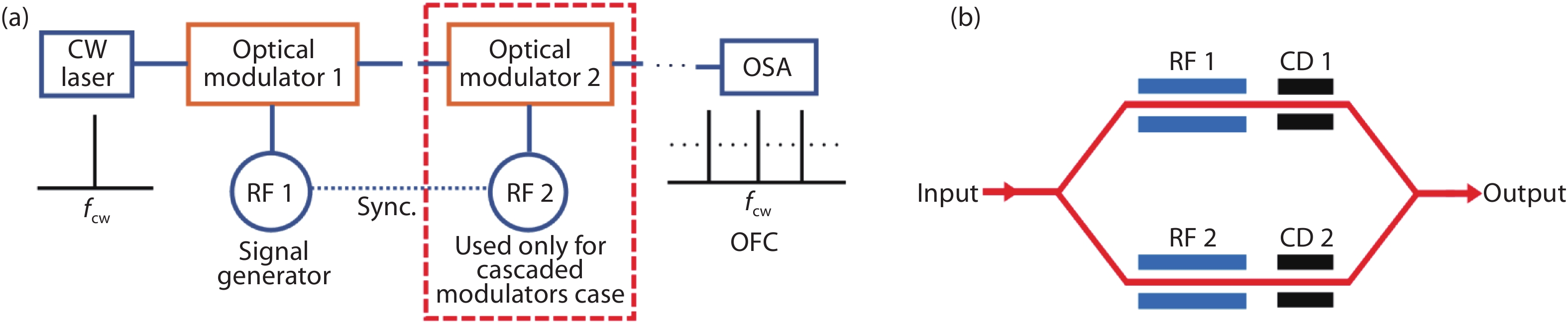
Three main components are used for EO OFC generation: a continuous wave (CW) laser, one or more EO modulators, and RF signal generator(s), see Fig. 1(a). The output spectrum is centered at the wavelength of the CW laser and for a single EO modulator, the comb spacing is determined by the RF signal generator. Cascading two or more EO modulators leads to a greater number of comb lines and correspondingly, a larger bandwidth. The number of comb lines is dependent on the modulation depth obtained in each modulator, which in turn depends on the operating conditions such as RF power and bias voltages.
![]()
Figure 1.(Color online) (a) Generic setup for OFC generation. (b) Schematic of a DD-MZM.
We assume a CW laser with a carrier frequency
where
with
where
For OFC generation using a general DD-MZM [see Fig. 1(b)], we assume two RF signal generators drive the upper and lower arms of the modulator at frequencies
where
Taking the Fourier transform of Eq. (5) gives the output signal in the frequency domain[
The corresponding amplitudes of the comb lines are determined by the Bessel functions and the voltages applied to the modulators. Note that for a single-drive MZM, we can set one of the driving voltages to
For the case of cascading an MZM with a PM, we can express the output electric field in the time domain as[
where
Intensity modulation in MRMs can be achieved through two means: (1) by modulating the ring waveguide (intracavity ring modulator) or (2) by modulating the coupling between the ring and the bus waveguides (coupling-modulated ring). When light propagates in the ring, it acquires a phase shift
Fig. 2 shows a schematic of an intracavity MRM and its transmission spectrum; the red line indicates the operating wavelength of the CW input for efficient modulation. The input wavelength should lie within the most linear region of the transmission response, as in the case of MZMs. The modulation efficiency increases as the resonance of the ring is deeper, i.e., a larger extinction ratio can be obtained. However, there is a trade-off between extinction ratio and modulation bandwidth[
![]()
Figure 2.(Color online) (a) Schematic of an intracavity MRM. (b) Transmission spectrum of an MRM (the input laser wavelength is shown in red for illustration).
Using coupled mode theory, we can express the transfer function of the MRM as follows[
where the parameters
where
Fig. 1(a) illustrates the generic setup for OFC generation using cascaded modulators; to understand the principle of operation, we consider only two cascaded modulators. The output from a CW laser is launched into the first modulator driven by an RF signal generator at frequency
When using IMs, there are several frequency conditions that relate
where Δf is the frequency spacing between the comb lines. Fig. 3 shows the possible OFC spectra corresponding to these three conditions. For example, if we use the condition specified in Eq. (11) and drive the first MZM at
![]()
Figure 3.(Color online) OFC generation using different driving conditions: (a)
It is also possible to generate OFCs using a cascade of PMs and IMs, e.g., 3 PMs and an IM, or cascading a DD-MZM and a PM. Of course, cascading three or more optical modulators leads to a more complex system which requires greater control over tuning the phase shifters between the modulators and proper adjustment of the driving RF power [
3. Integrated electro-optic comb generation
3.1. OFC generation in InP
The use of III–V materials, e.g., GaAs or InP, allows for the integration of all active components for on-chip EO OFC generation[
In Ref. [43], Slavík et al. realized a more compact OFC generator that comprised an integrated C-band tunable laser with a dual-electrode MZM in a single package. The output optical power of the tunable laser was 13 dBm while the total loss of the push-pull modulator was ~ 6 dB (including input/output coupling loss). The 3 dB bandwidth and
In Ref. [44], Andriolli et al. reported an InP-based OFC generator which integrated a tunable distributed Bragg reflector laser diode (DBR-LD), an MZM, two PMs, and a semiconductor optical amplifier (SOA) on a chip occupying an area of
![]()
Figure 4.(Color online) Schematic of the InP-based OFC generator in Refs. [
To increase the number of comb lines, Bontempi et al. exploited a dual-drive configuration[
3.2. OFC generation in LiNbO3
Lithium niobate is an excellent photonic material due to its advantages of large second order nonlinearity and ultrabroad transparent window from 350 to 5000 nm[
3.3. OFC generation in SOI
3.3.1. Microring modulators
Two setups commonly employed for OFC generation with MRMs are shown in Fig. 5. In Fig. 5(a), the output from two RF signal generators, one at f and the other at 2f, is used to drive a single MRM (the phase difference between the two RF signal generators is tuned using a phase shifter). In Fig. 5(b), two cascaded MRMs are used, each driven by a separate RF signal generator. In both cases, the OFC spectrum depends on the operating conditions as described in Section 2.
![]()
Figure 5.(Color online) Typical experimental setup for OFC generation using (a) single MRM, (b) cascaded MRMs.
In Ref. [34], a CMOS compatible process was used to fabricate an intracavity MRM. The microring had a radius of 14 μm and a coupling gap of 240 nm to the bus waveguide (for operation near the critical coupling point). The bus and ring waveguides had a width of 450 nm, a height of 220 nm, and a slab height of 90 nm. The waveguides were loaded with a PN junction implanted with phosphorus and boron to form N and P regions, respectively. For this design, a π phase shift could be obtained at critical coupling, which was achieved at a forward bias voltage of 1 V. An OFC with 5 comb lines, a comb spacing up to 10 GHz, and a flatness within 0.7 dB was obtained using a setup similar to that shown in Fig. 5(a).
In Ref. [47], an OFC comprising 12 comb lines with a comb spacing of 10 GHz was achieved using an MRM followed by a microring filter. The device was fabricated on a 220 nm SOI platform. A lateral PN junction was loaded on the circumference of the ring to deplete the free carriers. At zero bias voltage, the device had an extinction ratio of 20 dB (confirming operation near the critical coupling point). In reverse bias, the resonance exhibited a red-shift of ~ 27.5 pm/V. Both the MRM and microring filter were identical and designed with a radius of 7.5 μm and a coupling gap of 200 nm. The 3 dB bandwidth of the MRM was around 18 GHz. The microring filter was used to equalize the 5 middle lines.
In Ref. [48], Xu et al. proposed using cascaded MRMs for OFC generation using the frequency condition specified in Eq. (13). Both intracavity MRMs were identical, with a radius of 10 μm and a coupling gap of 315 nm. The lateral PN junctions covered 70% of the circumference, and the metal heater covered 95% of the circumference. The waveguides that form the microrings had a width of 500 nm, a height of 220 nm, and a slab height of 90 nm. When no bias voltage was applied, one MRM had an extinction ratio of 26 dB. The 3 dB bandwidth was measured to be about 25 GHz. Using a setup similar to that shown in Fig. 5(b) with RF signal generators at 20 and 10 GHz driving the first and second MRMs, respectively, they obtained an OFC with 5 comb lines, a comb spacing of 10 GHz, and a flatness within 8 dB.
We also investigated the use of cascaded MRMs for EO OFC generation[
![]()
Figure 6.(Color online) (a) Schematic of the proposed MRM. (b) Cross-section of the PN junction of the ring. (c) Microscopic image of one MRM. (d)
For OFC generation, we only focused on driving the PN junction (microring waveguide) with no voltage applied to the MMI. We start by identifying the DC characteristics of one MRM by applying forward bias and reverse bias in the PN junction as shown in Figs. 7(a) and 7(b), respectively. When there is no voltage applied to the microring, the device exhibits a deep resonance at around 1553.3 nm. Under forward bias, there is a blue-shift in the resonant wavelength since free carriers are injected into the PN junction causing a reduction in the refractive index. The opposite phenomenon occurs under reverse bias (red-shift). Fig. 6(d) shows the measured S11 and S21 responses of a single MRM; the 3 dB bandwidth normalized to the value at 1.5 GHz is ~ 5 GHz.
![]()
Figure 7.(Color online) Transmission spectrum of one MRM in (a) forward bias and (b) reverse bias.
Fig. 8(a) shows the experimental setup for OFC generation. We start by aligning the two ring’s resonances on top of each other and operate the CW laser on the most linear region as discussed in Section 2. When we use the operating conditions given in Eq. (11), i.e.,
![]()
Figure 8.(Color online) (a) Experimental setup. (b) Driving MRM 1 with 10 GHz and MRM 2 with 5 GHz. (c) Driving MRM 1 with 5 GHz and MRM 2 with 15 GHz. (d) Comb spectrum demonstrating 5 lines when driving MRM 1 at 20 GHz and MRM 2 at 10 GHz. (e) Temporal waveform of (b). (f) Temporal waveform of (c).
From the previous reported cases, the output frequency comb spectrum is limited by the 3 dB bandwidth of the MRM used. The comb amplitude variations are limited by the resonance steep (extinction ratio), namely, if the MRM operates in its critical coupling, the intensity at the resonance wavelength exhibit an abrupt π phase shift indicating a better modulation efficiency than over-coupling or under-coupling conditions. The number of comb lines depends on the frequency conditions used to drive the RF signal generators as discussed before.
3.3.2. Dual-drive MZMs
Recently Lin et al. explored the use of a single DD-MZM in SOI for EO OFC generation[
3.3.3. Cascaded MZMs
Fig. 9 shows the principle of OFC generation using cascaded MZMs, which is a generalization of Fig. 3 and the operating conditions specified in Eq. (11). As the DC bias of each MZM has an impact on the power level of each comb line, we can shape the spectral profile of the OFC by tuning the DC bias for each MZM. One important application of this schematic is to generate sinc-shaped Nyquist pulses, or correspondingly, an OFC with a rectangular spectral profile. Note that while it is possible to generate OFCs by cascading several PMs, especially to increase the number of comb lines, this comes at the expense of degraded sideband suppression[
![]()
Figure 9.(Color online) Schematic of cascaded MZMs for OFC generation.
Liu et al. demonstrated OFC generation using a cascaded MZM and PM[
![]()
Figure 10.(Color online) Schematic of integrated cascaded MZM and PM (after Ref. [
We have also demonstrated OFC and Nyquist pulse generation using two cascaded MZMs[
![]()
Figure 11.(Color online) Schematic of the OFC generator in silicon photonics.
Table Infomation Is Not EnableFor OFC generation, the CW light was injected into VGC 2 and a quasi-flat OFC can be obtained from VGC 1 by manipulating the heating voltages and reverse DC bias. Compared with the previous results in Ref. [53], we extended the comb spacing to 10 GHz (for an overall bandwidth up 90 GHz) with improved spectral flatness (see Fig. 12). In our experiments, we obtained comb spacings of 5, 7.5, and 10 GHz; the corresponding spectral flatness is 3.8, 4.7, and 6.5 dB, see Fig. 12. The flatness of the quasi-rectangular OFC degrades when the comb spacing is increased; higher RF power and the heater voltages need to be further optimized to improve the flatness. The corresponding temporal waveforms are shown in Fig. 12 and are in great agreement with ideal sinc-shaped Nyquist pulses (assuming a perfect rectangular OFC shape). The full width half maximums for the waveforms in Figs. 10(a), 10(b), and 10(c) are 17.6, 13.1, and 11.4 ps; the corresponding rms timing jitters are 1.2, 1.7, and 1.1 ps, respectively, showing the high quality of the generated pulses.
![]()
Figure 12.(Color online) Experimental results of the OFC in silicon photonics. (a–c) the OFCs with spacing from 5, 7.5, and 10 GHz; left: spectral profile; right: temporal signals.
4. Outlook
Integrated technologies for EO OFC generation have been attracting growing attention in recent years. A summary of results obtained using InP, LNOI, and SOI is given in Table 2.
One of the greatest advantages of using InP is the integration of optical sources with modulators, as well as optical amplifiers to increase the output power. Although only modest output powers (e.g., –4 dBm) have been reported to date, higher values should be possible, e.g., using booster SOA designs. Moreover, wavelength multiplexing of locked integrated multi-wavelength sources is possible thereby allowing for the generation of broadband combs for various applications such as Nyquist WDM transmission [
With SOI, while the number of comb lines demonstrated to date has been modest, the spectral flatness has been reasonable, corresponding to the generation of Nyquist pulses of high quality. Moreover, the comb spacing achieved is comparable to commercial LiNbO3 waveguide modulators. Silicon photonic modulators with bandwidths up to 45 GHz have been demonstrated[
Perhaps the most exciting development has been the realization of efficient EO phase shifters and modulators in LNOI. PMs with resonators can certainly achieve a very large number of comb lines albeit with a sloped amplitude response (i.e., limited spectral flatness). They have low insertion loss and are compact. It should also be possible to realize cascaded modulators thereby allowing for the generation of broadband OFCs with reasonable spectral flatness. Such OFCs can be used for Nyquist OTDM or Nyquist WDM transmission. They can also be combined with various passive devices, including microring resonators or Bragg grating devices[
Acknowledgements
This research was supported in part by the Natural Sciences and Engineering Research Council of Canada and the Fonds du Québec – Nature et Technologies. We thank M. Ma, R. Adams, K. Yim, X. Jin, R. Maram, B. Naghdi, A. Sarmani, M. Jacques, and D. V. Plant for their contributions.
References
[1]
[2] L E Hargrove, R L Fork, M A Pollack. Locking of He –Ne laser modes induced by synchronous intracavity modulation. Appl Phys Lett, 5, 4(1964).
[3] T W Hänsch. Nobel lecture: Passion for precision. Rev Mod Phys, 78, 1297(2006).
[4] J L Hall. Nobel lecture: Defining and measuring optical frequencies. Rev Mod Phys, 78, 1279(2006).
[5] T Udem, R Holzwarth, T W Hänsch. Optical frequency metrology. Nature, 416, 233(2002).
[6] M G Suh, Q F Yang, K Y Yang et al. Microresonator soliton dual-comb spectroscopy. Science, 354, 600(2016).
[7] A Dutt, C Joshi, X C Ji et al. On-chip dual-comb source for spectroscopy. Sci Adv, 4, e1701858(2018).
[8] M G Suh, K J Vahala. Soliton microcomb range measurement. Science, 359, 884(2018).
[9] T Wilken, G L Curto, R A Probst et al. A spectrograph for exoplanet observations calibrated at the centimetre-per-second level. Nature, 485, 611(2012).
[10] T Steinmetz, T Wilken, C Araujo-Hauck et al. Laser frequency combs for astronomical observations. Science, 321, 1335(2008).
[11] D T Spencer, T Drake, T C Briles et al. An optical-frequency synthesizer using integrated photonics. Nature, 557, 81(2018).
[12] W Liang, D Eliyahu, V S Ilchenko et al. High spectral purity Kerr frequency comb radio frequency photonic oscillator. Nat Commun, 6, 7957(2015).
[13] X Y Xu, J Y Wu, T G Nguyen et al. Advanced RF and microwave functions based on an integrated optical frequency comb source. Opt Express, 26, 2569(2018).
[14] V Torres-Company, A M Weiner. Optical frequency comb technology for ultra-broadband radio-frequency photonics. Laser Photonics Rev, 8, 368(2014).
[15] M Imran, P M Anandarajah, A Kaszubowska-Anandarajah et al. A survey of optical carrier generation techniques for terabit capacity elastic optical networks. IEEE Commun Surv Tutorials, 20, 211(2018).
[16] A E Willner, A Fallahpour, K H Zou et al. Optical signal processing aided by optical frequency combs. IEEE J Sel Top Quantum Electron, 27, 1(2021).
[17] J C Lin, H Sepehrian, Y L Xu et al. Frequency comb generation using a CMOS compatible SiP DD-MZM for flexible networks. IEEE Photonics Technol Lett, 30, 1495(2018).
[18] D J Jones, S A Diddams, J K Ranka et al. Carrier-envelope phase control of femtosecond mode-locked lasers and direct optical frequency synthesis. Science, 288, 635(2000).
[19] A Ortigosa-Blanch, J Mora, J Capmany et al. Tunable radio-frequency photonic filter based on an actively mode-locked fiber laser. Opt Lett, 31, 709(2006).
[20] M Zhang, B Buscaino, C Wang et al. Broadband electro-optic frequency comb generation in a lithium niobate microring resonator. Nature, 568, 373(2019).
[21] B Stern, X C Ji, Y Okawachi et al. Battery-operated integrated frequency comb generator. Nature, 562, 401(2018).
[22] T J Kippenberg, R Holzwarth, S A Diddams. Microresonator-based optical frequency combs. Science, 332, 555(2011).
[23] J S Levy, A Gondarenko, M A Foster et al. CMOS-compatible multiple-wavelength oscillator for on-chip optical interconnects. Nat Photonics, 4, 37(2010).
[24] A G Griffith, R K W Lau, J Cardenas et al. Silicon-chip mid-infrared frequency comb generation. Nat Commun, 6, 1(2015).
[25] T J Kippenberg, A L Gaeta, M Lipson et al. Dissipative Kerr solitons in optical microresonators. Science, 361, eaan8083(2018).
[26] X Yi, Q F Yang, K Y Yang et al. Soliton frequency comb at microwave rates in a high-Q silica microresonator. Optica, 2, 1078(2015).
[27] H J Chen, Q X Ji, H Wang et al. Chaos-assisted two-octave-spanning microcombs. Nat Commun, 11, 2336(2020).
[28] A Parriaux, K Hammani, G Millot. Electro-optic frequency combs. Adv Opt Photon, 12, 223(2020).
[29] I L Gheorma, G K Gopalakrishnan. Flat frequency comb generation with an integrated dual-parallel modulator. IEEE Photonics Technol Lett, 19, 1011(2007).
[30] Z Jiang, C B Huang, D E Leaird et al. Optical arbitrary waveform processing of more than 100 spectral comb lines. Nat Photonics, 1, 463(2007).
[31] R Wu, V R Supradeepa, C M Long et al. Generation of very flat optical frequency combs from continuous-wave lasers using cascaded intensity and phase modulators driven by tailored radio frequency waveforms. Opt Lett, 35, 3234(2010).
[32] M A Soto, M Alem, M Amin Shoaie et al. Optical sinc-shaped Nyquist pulses of exceptional quality. Nat Commun, 4, 2898(2013).
[33] C Weimann, P C Schindler, R Palmer et al. Silicon-organic hybrid (SOH) frequency comb sources for terabit/s data transmission. Opt Express, 22, 3629(2014).
[34] I Demirtzioglou, C Lacava, K R H Bottrill et al. Frequency comb generation in a silicon ring resonator modulator. Opt Express, 26, 790(2018).
[35] B Buscaino, M Zhang, M Lončar et al. Design of efficient resonator-enhanced electro-optic frequency comb generators. J Lightwave Technol, 38, 1400(2020).
[36] S Cordette, A Vedadi, M A Shoaie et al. Bandwidth and repetition rate programmable Nyquist sinc-shaped pulse train source based on intensity modulators and four-wave mixing. Opt Lett, 39, 6668(2014).
[37] M J Yu, C Wang, M Zhang et al. Chip-based lithium-niobate frequency combs. IEEE Photonics Technol Lett, 31, 1894(2019).
[38] T H Ren, M Zhang, C Wang et al. An integrated low-voltage broadband lithium niobate phase modulator. IEEE Photonics Technol Lett, 31, 889(2019).
[39] A Shams-Ansari, M J Yu, Z J Chen et al. Microring electro-optic frequency comb sources for dual-comb spectroscopy. CLEO: QELS_Fundamental Science, JTh5B. 8(2019).
[40]
[41]
[42] N Yokota, H Yasaka. Operation strategy of InP Mach–Zehnder modulators for flat optical frequency comb generation. IEEE J Quantum Electron, 52, 1(2016).
[43] R Slavík, S G Farwell, M J Wale et al. Compact optical comb generator using InP tunable laser and push-pull modulator. IEEE Photonics Technol Lett, 27, 217(2015).
[44] N Andriolli, T Cassese, M Chiesa et al. Photonic integrated fully tunable comb generator cascading optical modulators. J Lightwave Technol, 36, 5685(2018).
[45] F Bontempi, N Andriolli, F Scotti et al. Comb line multiplication in an InP integrated photonic circuit based on cascaded modulators. IEEE J Sel Top Quantum Electron, 25, 1(2019).
[46] K P Nagarjun, V Jeyaselvan, S K Selvaraja et al. Generation of tunable, high repetition rate optical frequency combs using on-chip silicon modulators. Opt Express, 26, 10744(2018).
[47]
[48] Y L Xu, J C Lin, R Dubé-Demers et al. Integrated flexible-grid WDM transmitter using an optical frequency comb in microring modulators. Opt Lett, 43, 1554(2018).
[49]
[50]
[51] Z F Wang, M Ma, H Sun et al. Optical frequency comb generation using CMOS compatible cascaded Mach–Zehnder modulators. IEEE J Quantum Electron, 55, 1(2019).
[52]
[53] S Q Liu, K Wu, L J Zhou et al. Optical frequency comb and nyquist pulse generation with integrated silicon modulators. IEEE J Sel Top Quantum Electron, 26, 1(2020).
[54] R Dubé-Demers, S LaRochelle, W Shi. Ultrafast pulse-amplitude modulation with a femtojoule silicon photonic modulator. Optica, 3, 622(2016).
[55] D Marpaung, C Roeloffzen, R Heideman et al. Integrated microwave photonics. Laser Photonics Rev, 7, 506(2013).
[56] Y Ogiso, J Ozaki, Y Ueda et al. Over 67 GHz bandwidth and 1.5 V vπ InP-based optical IQ modulator with n-i-p-n heterostructure. J Lightwave Technol, 35, 1450(2017).
[57] K A Williams, E A J M Bente, D Heiss et al. InP photonic circuits using generic integration. Photon Res, 3, B60(2015).
[58] F A Kish, D Welch, R Nagarajan et al. Current status of large-scale InP photonic integrated circuits. IEEE J Quantum Electron, 7, 1470(2011).
[59] M Bazzan, C Sada. Optical waveguides in lithium niobate: Recent developments and applications. Appl Phys Rev, 2, 040603(2015).
[60] R B Wu, M Wang, J Xu et al. Long low-loss-litium niobate on insulator waveguides with sub-nanometer surface roughness. Nanomaterials, 8, 910(2018).
[61] M Zhang, C Wang, R Cheng et al. Monolithic ultra-high-Q lithium niobate microring resonator. Optica, 4, 1536(2017).
[62] C Wang, M Zhang, X Chen et al. Integrated lithium niobate electro-optic modulators operating at CMOS-compatible voltages. Nature, 562, 101(2018).
[63] M B He, M Y Xu, Y X Ren et al. High-performance hybrid silicon and lithium niobate Mach–Zehnder modulators for 100 Gbit s−1 and beyond. Nat Photonics, 13, 359(2019).
[64] D X Xu, A Densmore, P Waldron et al. High bandwidth SOI photonic wire ring resonators using MMI couplers. Opt Express, 15, 3149(2007).
[65] M Jacques, Z P Xing, A Samani et al. 240 gbit/s silicon photonic Mach-Zehnder modulator enabled by two 2.3-Vpp drivers. J Lightwave Technol, 38, 2877(2020).
[66] D Pérez, I Gasulla, J Capmany. Programmable multifunctional integrated nanophotonics. Nanophotonics, 7, 1351(2018).
[67] M A Baghban, J Schollhammer, C Errando-Herranz et al. Bragg gratings in thin-film LiNbO3 waveguides. Opt Express, 25, 32323(2017).
[68]


Set citation alerts for the article
Please enter your email address

© Copyright 2018-2021 | Chinese Laser Press. All Rights Reserved 沪ICP备15018463号-20