• Photonics Research
  • Vol. 10, Issue 9, 2081 (2022)
Chunhui Yao1, Qixiang Cheng1、*, Günther Roelkens2, and Richard Penty1
Author Affiliations
  • 1Centre for Photonic Systems, Electrical Engineering Division, Department of Engineering, University of Cambridge, Cambridge CB3 0FA, UK
  • 2Department of Information Technology (INTEC), Photonics Research Group, Ghent University-imec, 9052 Ghent, Belgium
  • show less
    DOI: 10.1364/PRJ.465765 Cite this Article Set citation alerts
    Chunhui Yao, Qixiang Cheng, Günther Roelkens, Richard Penty. Bridging the gap between resonance and adiabaticity: a compact and highly tolerant vertical coupling structure[J]. Photonics Research, 2022, 10(9): 2081 Copy Citation Text show less
    (a) Schematic of the cross section of a III-V-on-silicon vertically coupled waveguide system. (b)–(d) Calculated maps of γ for different width combinations of the III-V and Si waveguide when the misalignment is 0, 0.5, and 1.0 μm, respectively. The dashed white lines and the orange dots represent the width combinations for, respectively, the linearly tapered structure and the multisegmented tapered structure.
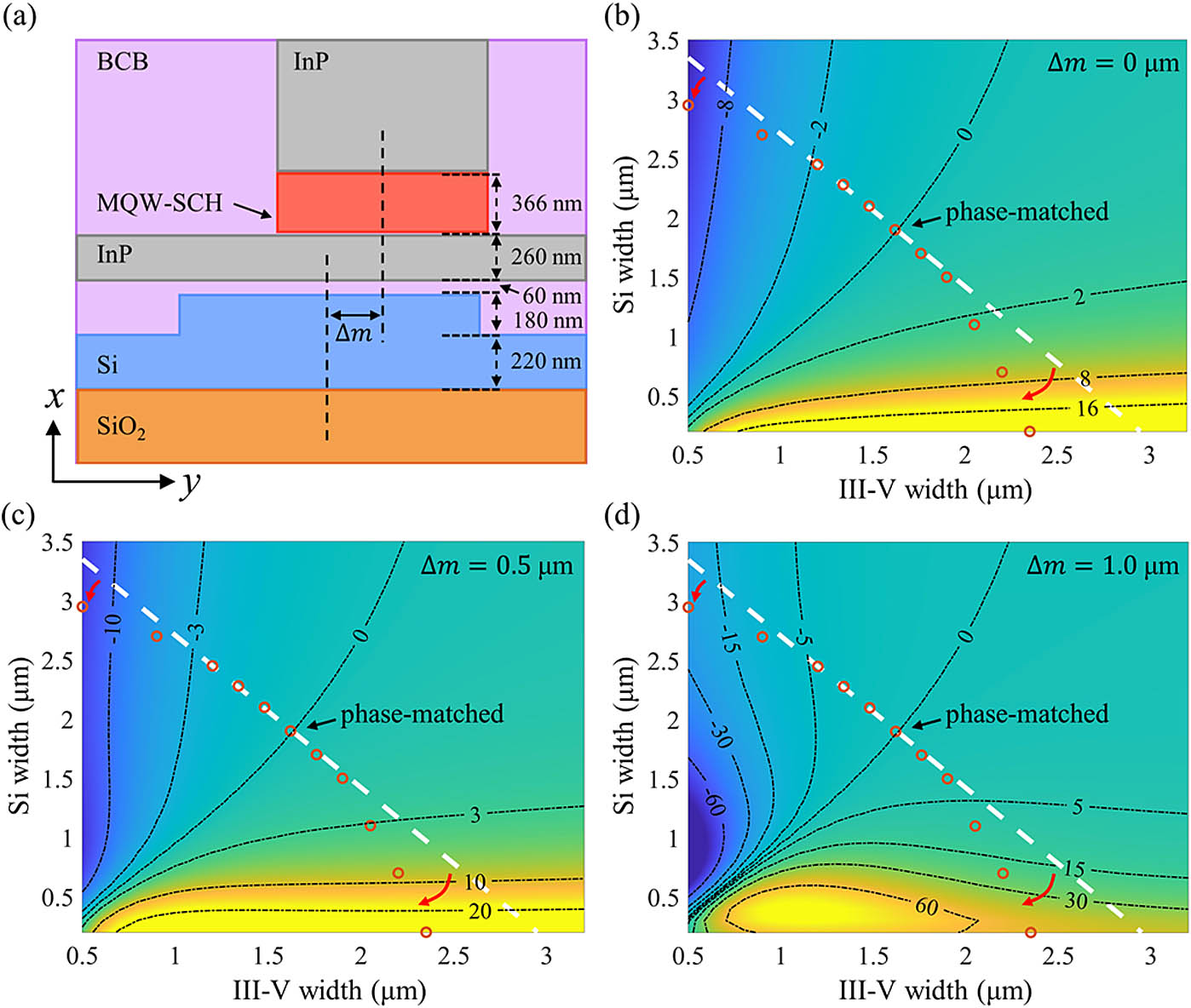
    Fig. 1. (a) Schematic of the cross section of a III-V-on-silicon vertically coupled waveguide system. (b)–(d) Calculated maps of γ for different width combinations of the III-V and Si waveguide when the misalignment is 0, 0.5, and 1.0 μm, respectively. The dashed white lines and the orange dots represent the width combinations for, respectively, the linearly tapered structure and the multisegmented tapered structure.
    (a) 3D schematic diagram of the proposed III-V-on-silicon vertical coupler. (b) and (c) Top view of the vertical couplers with, respectively, a linear taper structure and a multisegmented taper structure.
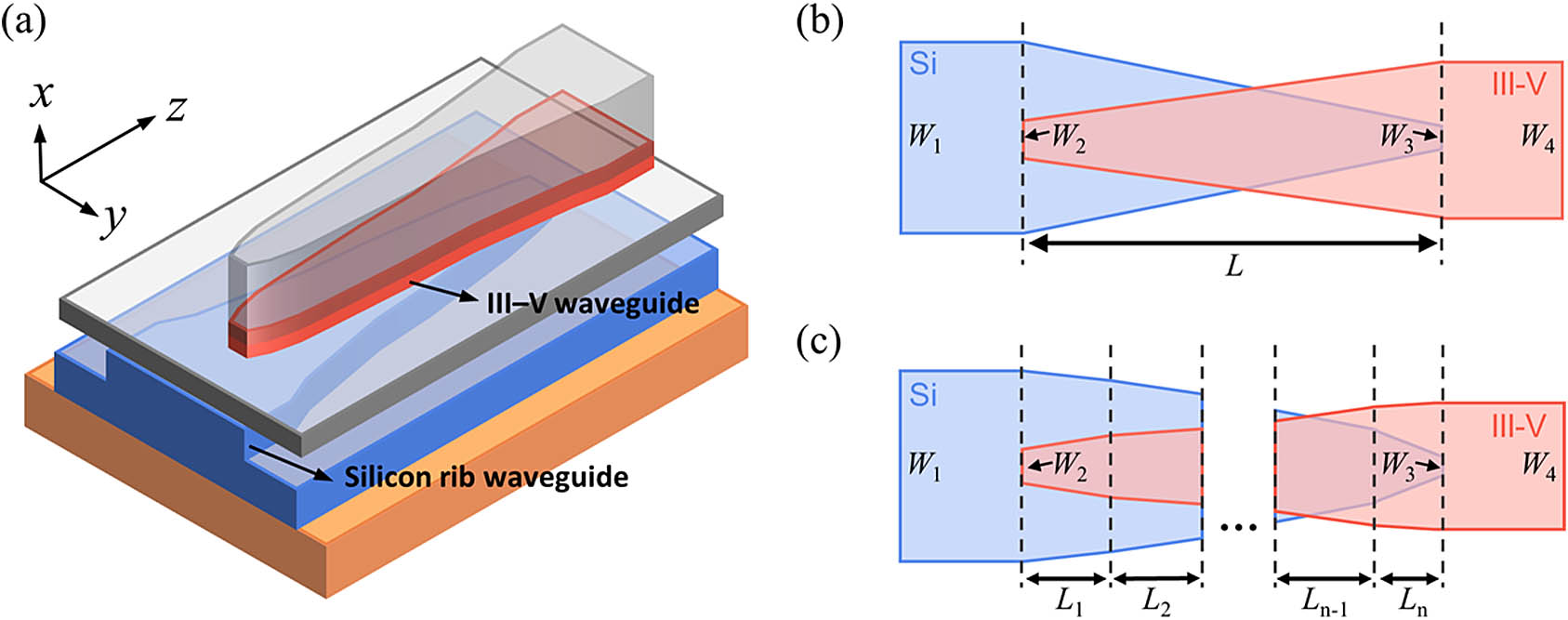
    Fig. 2. (a) 3D schematic diagram of the proposed III-V-on-silicon vertical coupler. (b) and (c) Top view of the vertical couplers with, respectively, a linear taper structure and a multisegmented taper structure.
    Simulated coupling efficiency versus the length L of the linear taper vertical couplers with different lateral misalignments. The theoretical calculation for a perfectly phase-matched conventional resonant coupler when Δm is 1.0 μm is also presented for reference.
    Fig. 3. Simulated coupling efficiency versus the length L of the linear taper vertical couplers with different lateral misalignments. The theoretical calculation for a perfectly phase-matched conventional resonant coupler when Δm is 1.0 μm is also presented for reference.
    (a) Waveguide widths of the vertical coupler with multisegmented taper structure along the propagation direction z. (b) Simulated coupling efficiency versus the lateral misalignment. (c) Normalized power of the two supermodes (even and odd) along the propagation direction when Δm is 1.0 μm. Insets show their simulated transverse electric field profiles at z=57 μm. (d) Simulated electric field profiles at the input cross section and the output cross section when Δm is, respectively, 0, 0.5, and 1.0 μm.
    Fig. 4. (a) Waveguide widths of the vertical coupler with multisegmented taper structure along the propagation direction z. (b) Simulated coupling efficiency versus the lateral misalignment. (c) Normalized power of the two supermodes (even and odd) along the propagation direction when Δm is 1.0 μm. Insets show their simulated transverse electric field profiles at z=57  μm. (d) Simulated electric field profiles at the input cross section and the output cross section when Δm is, respectively, 0, 0.5, and 1.0 μm.
    (a) Simulated map of the coupling efficiency with different width variations of the III-V and Si waveguide when the coupler is 1.0 μm misaligned. (b) Simulated coupling efficiency versus the thickness of the BCB bonding layer with different misalignments. (c) Simulated coupling efficiency versus wavelength with different misalignments.
    Fig. 5. (a) Simulated map of the coupling efficiency with different width variations of the III-V and Si waveguide when the coupler is 1.0 μm misaligned. (b) Simulated coupling efficiency versus the thickness of the BCB bonding layer with different misalignments. (c) Simulated coupling efficiency versus wavelength with different misalignments.
    (a) Cross section schematic of a heterogenous coupled waveguide system based on 220 nm SOI platform with poly-Si overlay. (b) Waveguide widths of the multisegmented vertical coupler along the propagation direction. (c) FDTD simulated coupling efficiency versus the lateral misalignment.
    Fig. 6. (a) Cross section schematic of a heterogenous coupled waveguide system based on 220 nm SOI platform with poly-Si overlay. (b) Waveguide widths of the multisegmented vertical coupler along the propagation direction. (c) FDTD simulated coupling efficiency versus the lateral misalignment.
    Simulated coupling efficiency of the optimized couplers with different numbers of taper segments when Δm is ±1.0 μm. Inset shows the coupling efficiency of a three-segmented coupler versus the lateral misalignment.
    Fig. 7. Simulated coupling efficiency of the optimized couplers with different numbers of taper segments when Δm is ±1.0  μm. Inset shows the coupling efficiency of a three-segmented coupler versus the lateral misalignment.
    ReferencesPrincipleMaterialsLengthEfficiencyAlignment ToleranceTolerance of Width Variation (>80%)Bandwidth
    [23]AdiabaticAlGaInAs/Si210 μm98%±1.0  μm (>93%)N.A.N.A.
    [43]AdiabaticInGaAsP/a-Si:H224 μm93%±1.0  μm (>75%)N.A.N.A.
    [39]AdiabaticInGaAsP/InP180 μm83%N.A.±0.4  μmN.A.
    [40]AdiabaticInGaAsP/InP293 μm90%N.A.±0.125  μmN.A.
    [34]ResonantAlGaInAs/Si8 μm95%±0.1  μm (>90%)N.A.1.5–1.6 μm (>95%)
    [35]ResonantAlGaInAs/Si5 μm98%N.A.N.A.1.5–1.6 μm (>90%)
    [32]ResonantInGaAsP/InP24 μm97%N.A.±0.125  μmN.A.
    [44]ResonantAlGaInAs/InP55 μm96%±0.3  μm (>90%)±0.25  μm1.23–1.4 μm (>80%)
    This workHybridAlGaInAs/Si87 μm98%±1.0  μm (>94%)±0.5  μm1.44–1.74 μm (>90%)
    Table 1. Comparison of Several Different Vertical Couplersa
    Performance MetricsAdiabatic CouplerMultisegmented Tapered Coupler
    Device length237 μm87 μm
    Alignment tolerance1.0 μm (>91%)1.0 μm (>94%)
    Tolerance of width variation±0.3  μm (>75%)±0.5  μm (>80%)
    Tolerance of BCB thickness variation±10nm (>86%)±50nm (>90%)
    Bandwidth1.49–1.58 μm (>90%)1.44–1.74 μm (>90%)
    Table 2. Comparison to an Adiabatic Coupler
    Chunhui Yao, Qixiang Cheng, Günther Roelkens, Richard Penty. Bridging the gap between resonance and adiabaticity: a compact and highly tolerant vertical coupling structure[J]. Photonics Research, 2022, 10(9): 2081
    Download Citation