
Chunhui Yao, Qixiang Cheng, Günther Roelkens, Richard Penty, "Bridging the gap between resonance and adiabaticity: a compact and highly tolerant vertical coupling structure," Photonics Res. 10, 2081 (2022)
- Photonics Research
- Vol. 10, Issue 9, 2081 (2022)
Abstract
1. INTRODUCTION
Photonic integrated circuit (PIC) technology powers the modern internet, enabling video conferences, data analytics, and cloud-based services [1,2]. A sustained reduction in size and costs for PICs is also enabling game-changing innovations in a host of new sectors, such as sensing [3] and information processing [4]. Silicon photonics, which leverages the developed technologies in CMOS manufacturing, has been developed in both academia and industry, providing a low-cost platform for compact and low-loss photonic integration [5]. However, since making on-chip light sources out of silicon is still a long way from being practical due to its indirect bandgap [6], reliable integration of III-V gain materials into the silicon photonics platform at the wafer level is an essential requirement for future silicon photonics products. Over the past decade, intensive efforts have been made to facilitate III-V-on-silicon devices; e.g., semiconductor optical amplifiers (SOAs) [7,8], photodetectors [9,10], and lasers [11,12], using different approaches that include hetero-epitaxial growth [13,14], flip-chip integration [15,16], and die/wafer-to-wafer bonding [17,18]. In recent years, microtransfer printing (μTP) technology appeared as a newcomer in the field of heterogenous integration [19]. By parallel transfer printing prefabricated micron-sized III-V components onto the silicon PICs, μTP combines the advantages of flip-chip integration (pretesting of the III-V devices) and wafer bonding (high throughput integration) [20] without disturbing the backend flow of silicon photonics, paving a promising way toward efficient wafer-scale III-V-on-silicon integration. The
Vertical couplers that complete the optical power transfer between the III-V and silicon layers are the key components for heterogeneously integrated devices. Through slow changes in geometry, adiabatic couplers can achieve high alignment tolerance, yet at the cost of large footprint (e.g., about 500 μm each pair in Ref. [23]), being prohibitively long for complex PICs that incorporate a large number of active components. This is particularly pronounced for applications such as large-scale optical switch fabrics [24,25] and optical information processors [26,27], where massive arrays of III-V components are densely integrated at the chip level. Alternatively, resonant couplers based on the periodic mode beating feature compact lengths, but are rather intolerant to misalignments or fabrication variations [28,29]. Therefore, a new coupler design that combines the high alignment tolerance of adiabatic couplers and the compactness of resonant couplers is desired.
In this work, we propose a design method for a compact, highly tolerant vertical coupler for building dense heterogeneous PICs. Based on inversely tapered structures with careful geometrical optimization, our design allows a certain proportion of the odd supermode to be excited during the coupling process, which helps break the sensitive dependence on the coupling length that resonant couplers always suffer from and enables a compact length of only 87 μm, being almost threefold shorter than the state-of-the-art alignment-tolerant adiabatic coupler [23]. A finite-difference time-domain (FDTD) simulation shows that its coupling efficiency reaches 98% (i.e., 0.1 dB coupling loss) when perfectly aligned and maintains more than 94% (
Sign up for Photonics Research TOC. Get the latest issue of Photonics Research delivered right to you!Sign up now
This paper has six sections. Section 2 reviews different vertical coupling schemes along with their advantages and disadvantages. The theoretical analysis is described in Section 3 with insights on how to relax the alignment tolerance. Section 4 presents the methodology of the coupler design and optimization where we first propose a sharp linear taper structure, and then extend that to a multisegmented taper structure with varying slopes to improve the performance. Section 5 provides further simulation results and discussions. Finally, we draw conclusions in Section 6.
2. REVIEW OF VERTICAL COUPLING STRATEGIES
Based on the different behavior of the supermodes (i.e., the odd and even modes) in the coupled mode system, current vertical couplers can be divided into two categories: resonant and adiabatic couplers [30,31]. Resonant couplers are based on a periodic interference phenomenon between the two supermodes so that, by setting the coupling region to be half of the mode beating length, optical power would be transferred from one waveguide to the other [28,29]. In this way, couplers can be made with short lengths [32], but have a drawback: their coupling efficiency is sensitive to fabrication variations since any slight structural deformation of the waveguides would influence the beating length and the profiles of the supermodes [33]. Recently, ultracompact resonant couplers have been predicted with a length of several microns, but their narrow waveguide widths (small feature sizes) and poor structural tolerances would impose rigorous demands on fabrication techniques [34,35]. Adiabatic couplers, on the contrary, are designed to keep the optical power in the fundamental mode (i.e., only even mode exists). By gradually increasing the optical confinement factor in the target waveguide through slow changes in the device geometry, the full optical power transfer can be eventually accomplished at the output end [36]. Adiabatic coupling does not require strict fabrication and alignment control; therefore, it has become the preferred choice [37,38]. Nevertheless, it naturally requires a rather long length to satisfy the adiabatic condition [39,40], which significantly limits the integration density. Though some approaches have been proposed to realize so-called “shortcuts to the adiabaticity” targeting to reduce the lengths of adiabatic couplers, they may not be suitable for the design of heterogeneous vertical couplers since the gap between the III-V and silicon layers is not manipulatable [41]. Moreover, these approaches may still result in hundreds of microns in length. For example, in Ref. [42], researchers theoretically derived the design criterion for the shortest adiabatic couplers. This criterion was later applied in Ref. [23] to realize alignment-tolerant adiabatic vertical couplers, which, however, are more than 200 μm long.
Table 1 summarizes the simulated results for state-of-the-art vertical couplers, highlighting their key metrics, from which the strengths and weaknesses for resonant or adiabatic couplers are clearly compared. Hence, to bridge the performance gap between adiabatic and resonant couplers, we propose a new compact and alignment/fabrication-tolerant vertical coupler design. Unlike a conventional resonant coupler, which initially excites both even and odd modes or an adiabatic coupler that does not excite odd mode at all times, our design operates in a hybrid way so that the even mode plays a dominant role while the odd mode is also partially excited in the central region of the coupler; hence, the design features the advantages of both resonant and adiabatic coupling. It can be seen from Table 1 that our proposed coupler has the best alignment and fabrication tolerance (even superior to those adiabatic couplers) and keeps a sub-hundred-micron length. In the following sections, we will present a detailed explanation of our design.
Comparison of Several Different Vertical Couplers
| References | Principle | Materials | Length | Efficiency | Alignment Tolerance | Tolerance of Width | Bandwidth |
|---|---|---|---|---|---|---|---|
| [ | Adiabatic | AlGaInAs/Si | 210 μm | 98% | N.A. | N.A. | |
| [ | Adiabatic | InGaAsP/a-Si:H | 224 μm | 93% | N.A. | N.A. | |
| [ | Adiabatic | InGaAsP/InP | 180 μm | 83% | N.A. | N.A. | |
| [ | Adiabatic | InGaAsP/InP | 293 μm | 90% | N.A. | N.A. | |
| [ | Resonant | AlGaInAs/Si | 8 μm | 95% | N.A. | 1.5–1.6 μm ( | |
| [ | Resonant | AlGaInAs/Si | 5 μm | 98% | N.A. | N.A. | 1.5–1.6 μm ( |
| [ | Resonant | InGaAsP/InP | 24 μm | 97% | N.A. | N.A. | |
| [ | Resonant | AlGaInAs/InP | 55 μm | 96% | 1.23–1.4 μm ( | ||
| This work | Hybrid | AlGaInAs/Si | 87 μm | 98% | 1.44–1.74 μm ( |
This table shows simulation results.
3. RELAXING ALIGNMENT TOLERANCE
Figure 1(a) shows the transverse section of an exemplary III-V-on-silicon (Si) heterogeneously integrated system, which is a typical structure for optical amplifiers or lasers [17,23,43]. The III-V active region consists of six AlGaInAs multiple-quantum wells (MQWs) sandwiched by seven barriers together with a pair of separate confinement heterostructure (SCH) layers on both sides. To simplify the analysis, the III-V active region is considered to have a total thickness of 366 nm with an overall averaged refractive index of about 3.35 at 1550 nm [44]. The InP separation layer is 260 nm thick while the lower Si rib waveguide has a thickness of 400 nm with an etch depth of 180 nm. A 60 nm thick divinylsiloxane-bis-benzocyclobutene (BCB, refractive index of 1.56) bonding layer is assumed between the III-V and Si waveguide, as commonly used in μTP or die/wafer bonding processes [23,45]. Note that using a thinner BCB bonding layer can help increase the coupling strength between the upper and lower waveguides, and thereby shorten the coupling length. However, it happens at the expense of reducing the optical confinement in the III-V active region, which consequently compromises the gain efficiency [46]. A lateral misalignment between the III-V and Si waveguide is considered, denoted by
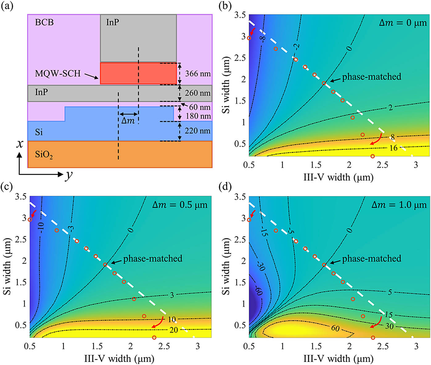
Figure 1.(a) Schematic of the cross section of a III-V-on-silicon vertically coupled waveguide system. (b)–(d) Calculated maps of
The structure in Fig. 1(a) can be regarded as an asymmetric vertically coupled waveguide system in which the propagation and interaction of optical modes can be approximately described by the coupled mode theory. The coupled equation can be written as [48,49]
Thus, to design a conventional resonant coupler for complete power transfer, its length should be set as half of the mode beating period, while the widths of both III-V and Si waveguides must be carefully selected to ensure that
![]()
Figure 2.(a) 3D schematic diagram of the proposed III-V-on-silicon vertical coupler. (b) and (c) Top view of the vertical couplers with, respectively, a linear taper structure and a multisegmented taper structure.
4. DEVICE DESIGN AND OPTIMIZATION
A. Vertical Coupler with Sharp Linear Taper Structure
As shown in Fig. 2(b),
We first choose the combination of widths
![]()
Figure 3.Simulated coupling efficiency versus the length
B. Vertical Coupler with a Multisegmented Taper Structure
As demonstrated above, a sharp taper structure can break the periodical mode coupling and hence can help improve the alignment tolerance. However, as the waveguide widths in a tapered structure inevitably vary along the propagation direction, it is difficult to maintain the phase matching between the upper and lower waveguides, particularly for the linearly tapered couplers since their slopes are fixed such that the phase matching is only satisfied at one specific point in the middle and rapidly deteriorates toward both ends. Thus, to achieve a better trade-off between the phase-matched and mismatched regions, numerous tapered segments with different slopes and lengths are required. Specifically, such a multisegmented taper structure shall have these features: (i) at its central part where the phase matching can be reasonably satisfied (i.e., where
In practice, we first choose the width combinations for all the segments, and then optimize their lengths based on the EME method. The orange dots in Figs. 1(b)–1(d) represent the chosen width combinations so that every two adjacent dots correspond to one specific segment. In the central region near the phase-matched point, the distribution of dots follows the optimal result of the sharp linear taper structure (i.e., located on the white dashed lines). At both sides of the coupler, the selection of dots is slightly adjusted to obtain smaller waveguide widths for two reasons: (i) to result in smaller values of
Because the design process we adopted here is straightforward (i.e., select the widths and then optimize the lengths), the PSO algorithm is powerful enough. Besides, it is possible to develop a feedback loop based on the outcomes of the optimization algorithm and adjust the initial selection of width combinations accordingly to further optimize the performance. Such a strategy can be potentially realized by more advanced algorithms, including machine learning or deep learning models [55,56], but may require significant computational resources and is beyond the scope of this paper.
Figure 4(a) shows the optimized geometry of the vertical coupler with numerous tapered segments. The total length is 87 μm. Notably, the segments around the phase-matched point (which is almost at the midpoint of the device) have smaller slopes than those segments on the two ends, which agrees with our previous analysis. A 3D FDTD method (Lumerical FDTD solver) is also used to provide more accurate results in addition to the EME method. Figure 4(b) shows the simulated coupling efficiency with different lateral misalignment, which indicates that the coupling efficiency is 98% (i.e.,
![]()
Figure 4.(a) Waveguide widths of the vertical coupler with multisegmented taper structure along the propagation direction
To reveal the underlying mode coupling behavior in our design, the power fraction carried by both the even and odd modes is monitored along the propagation direction, as shown in Fig. 4(c). It can be seen that at the beginning of the coupler, the optical power is adiabatically confined to the even mode and that barely any odd mode exists, while in the middle region with reasonable phase matching (between about 25 and 70 μm), a partial resonance phenomenon appears so that the odd mode is gradually excited and then coupled back to the even mode, with a peak value of 0.18. This clearly distinguishes our design from conventional resonant or adiabatic couplers. Figure 4(d) shows the simulated electric field profiles at the input and output cross sections, demonstrating that the optical power can be almost completely transferred from the lower Si waveguide to the upper III-V even with a
5. FURTHER PERFORMANCE EXPLORATION AND DISCUSSION
A. Tolerance of Structural Deformation
Besides the alignment tolerance, by simultaneously varying the widths of both upper III-V and lower Si waveguides, the level of tolerance for the width deviations of our design is investigated. Meanwhile, the impact of the thickness variations of the BCB bonding layer (i.e., the gap distance between the III-V and Si waveguide) as well as the silicon waveguide is also explored. Figure 5(a) shows that, on top of a 1.0 μm misalignment, when the width variations of the III-V and Si waveguide range from about
![]()
Figure 5.(a) Simulated map of the coupling efficiency with different width variations of the III-V and Si waveguide when the coupler is 1.0 μm misaligned. (b) Simulated coupling efficiency versus the thickness of the BCB bonding layer with different misalignments. (c) Simulated coupling efficiency versus wavelength with different misalignments.
The tolerance for the thickness variation of the BCB bonding layer is shown in Fig. 5(b). While the designed thickness of the BCB layer is 60 nm, the coupling efficiency keeps higher than 90% with the thickness varying from 50 to 65 nm when
B. Wavelength Dependence
The wavelength dependence of our proposed coupler is also studied, with the index dispersion of different material layers taken into consideration [58]. Figure 5(c) shows that a more than 90% coupling efficiency can be achieved over an ultrabroad wavelength band from 1.44 to 1.74 μm even with a 0.5 μm misalignment, which outperforms the other designs listed in Table 1. When the misalignment reaches 1.0 μm, the coupling efficiency still remains higher than 90% with the wavelength ranging from 1.52 to 1.61 μm.
C. Performance Comparison with Adiabatic Couplers
To highlight the superiority of our design, a direct comparison is made against an adiabatic coupler designed and simulated using the identical III-V-on-silicon coupled waveguide system [i.e., Fig. 1(a)] with a 1.0 μm misalignment. To achieve the theoretically shortest length, this adiabatic coupler follows the design criterion proposed in Ref. [42], as
Table 2 lists the comparison of the key performance metrics, showing that the adiabatic coupler can accomplish a similarly
Comparison to an Adiabatic Coupler
| Performance Metrics | Adiabatic Coupler | Multisegmented Tapered Coupler |
|---|---|---|
| Device length | 237 μm | 87 μm |
| Alignment tolerance | 1.0 μm ( | 1.0 μm ( |
| Tolerance of width variation | ||
| Tolerance of BCB thickness variation | ||
| Bandwidth | 1.49–1.58 μm ( | 1.44–1.74 μm ( |
D. Adoption on 220 nm SOI Platforms
As is widely acknowledged, it is nontrivial to directly couple the light from 220 nm Si waveguides (an effective index of about 2.45 with 0.5 μm width) into III-V active waveguides (an effective index of about 2.94 with 1.0 μm width) due to the large difference in index. To tackle this problem, efforts have been made either to reduce the effective index of a III-V waveguide, e.g., by developing ultrathin membrane III-V stacks [59], designing multisectional tapers with the thickness of the p-InP cladding layer lessened [35]; or to use the 400 or 500 nm thick SOI platforms for greater effective index (about 2.95 and 3.03, respectively, when the width is 0.6 μm) [60]. However, these methods may require extra or customized fabrication steps. In contrast, some foundries provide additional polycrystalline silicon (poly-Si) or amorphous silicon layers on top of the 220 nm Si layer as standard procedures, which can be used to thicken the passive waveguide for the vertical coupling at a lower cost and complexity. Thus, we take the imec iSiPP25G 220 nm SOI platform (commercially accessible through multiproject wafer runs) as an example [61]. The iSiPP25G platform offers a 180 nm poly-Si overlay, allowing the mode to exist within the Si and poly-Si joint waveguide. Figure 6(a) shows a heterogeneous coupled waveguide system based on it. Following the design method discussed in previous sections, we determine the geometry of the multisegmented vertical taper, as shown in Fig. 6(b). The overall length is 98.8 μm, which is slightly longer than our design based on the 400 nm SOI since the index matching is relatively compromised, but still achieves a sub-hundred-micron record. Figure 6(c) presents its misalignment tolerance showing that an over 91% coupling efficiency is obtained even when
![]()
Figure 6.(a) Cross section schematic of a heterogenous coupled waveguide system based on 220 nm SOI platform with poly-Si overlay. (b) Waveguide widths of the multisegmented vertical coupler along the propagation direction. (c) FDTD simulated coupling efficiency versus the lateral misalignment.
E. Design Considerations on Other Platforms
Whilst the proposed coupler is primarily for coupling between material layers with similar refractive indices, it is also possible to implement it in platforms with large index contrast. One example is the SiN-on-Si platforms, where people tend to use adiabatic coupling to overcome the index mismatch between the SiN and Si layers [62,63]. It is, however, possible to apply a subwavelength grating structure to reduce the effective index of the Si waveguide [64], thereby enabling the index matching in the proposed coupling mechanism. Another example is the μTP-based III-V-on-SiN platform. Due to the large difference in refractive index between III-V semiconductors and SiN, an additional poly-Si or amorphous Si layer can be used as an intermediate layer [43,65], in which our design method can be adopted.
Our design also can be applied to monolithic InP platforms based on the asymmetric twin guide (ATG) technique, where the active and passive waveguides are separated vertically [44,66]. Since the active and passive waveguides share similar refractive indices (e.g., InGaAsP or AlGaInAs layers with different composition and doping level), our design method can naturally fit.
F. Optimal Number of Taper Segments
Referring back to Section 4.B, a larger number of taper segments could in principle help achieve superior tolerance since the index matching can be better satisfied. Nevertheless, optimizing a larger number of taper segments could impose a heavier computational burden. Thus, to further explore the impact of segment number on the coupling performance, we simulated designs with different numbers of segments in the case of III-V-on-silicon coupling following the same design steps.
Figure 7 shows that at
![]()
Figure 7.Simulated coupling efficiency of the optimized couplers with different numbers of taper segments when
6. CONCLUSION
In this paper, we present a generic design method for a compact and alignment-tolerant vertical coupler for densely integrated III-V-on-silicon photonic circuits. Our coupler’s operation is fundamentally different from conventional resonant or adiabatic couplers that a certain proportion of the odd supermode is excited during the coupling process, enabling both high tolerance and compact length. The coupler structure contains numerous tapered segments, of which the start/end width combinations are determined based on the coupled mode theory, while the lengths are optimized using the PSO algorithm. The device length is 87 μm, which is almost threefold shorter than the state-of-the-art alignment-tolerant adiabatic coupler. Simulation results show that the designed coupler can achieve a 98% coupling efficiency (i.e., 0.1 dB insertion loss) when perfectly aligned and a
This work overcomes the limitations that conventional resonant couplers suffer from weak alignment and fabrication tolerance while adiabatic couplers are always too long, pointing to a new direction for the design of high-performance vertical couplers. Our proposed method also can be applied to different material systems; therefore, it is expected to find wide applications on various integration platforms.
Acknowledgment
Acknowledgment. The authors thank Mr. Peng Bao for his assistance in optical simulations. This project has received funding from the European Union’s Horizon 2020 research and innovation programme, project INSPIRE, and from the UK EPSRC Research, project QUDOS.
References
[1] F. Kish, V. Lal, P. Evans, S. W. Corzine, M. Ziari, T. Butrie, M. Reffle. System-on-chip photonic integrated circuits. IEEE J. Sel. Top. Quantum Electron., 24, 6100120(2017).
[2] Q. Cheng, M. Bahadori, M. Glick, S. Rumley, K. Bergman. Recent advances in optical technologies for data centers: a review. Optica, 5, 1354-1370(2018).
[3] S. Arafin, L. A. Coldren. Advanced InP photonic integrated circuits for communication and sensing. IEEE J. Sel. Top. Quantum Electron., 24, 6100612(2017).
[4] K. Kitayama, M. Notomi, M. Naruse, K. Inoue, S. Kawakami, A. Uchida. Novel frontier of photonics for data processing—photonic accelerator. APL Photon., 4, 90901(2019).
[5] Y. Su, Y. Zhang, C. Qiu, X. Guo, L. Sun. Silicon photonic platform for passive waveguide devices: materials, fabrication, and applications. Adv. Mater. Technol., 5, 1901153(2020).
[6] N. T. Otterstrom, R. O. Behunin, E. A. Kittlaus, Z. Wang, P. T. Rakich. A silicon Brillouin laser. Science, 360, 1113-1116(2018).
[7] M. L. Davenport, S. Skendžić, N. Volet, J. C. Hulme, M. J. R. Heck, J. E. Bowers. Heterogeneous silicon/III–V semiconductor optical amplifiers. IEEE J. Sel. Top. Quantum Electron., 22, 78-88(2016).
[8] G.-H. Duan, S. Olivier, S. Malhouitre, A. Accard, P. Kaspar, G. Valicourtde, G. Levaufre, N. Girard, A. LiepvreLe, A. Shen, D. Make. New advances on heterogeneous integration of III–V on silicon. J. Lightwave Technol., 33, 976-983(2015).
[9] S. Feng, Y. Geng, K. M. Lau, A. W. Poon. Epitaxial III-V-on-silicon waveguide butt-coupled photodetectors. Opt. Lett., 37, 4035-4037(2012).
[10] R. Wang, A. Vasiliev, M. Muneeb, A. Malik, S. Sprengel, G. Boehm, M. C. Amann, I. Šimonytė, A. Vizbaras, K. Vizbaras, R. Baets. III–V-on-silicon photonic integrated circuits for spectroscopic sensing in the 2–4 μm wavelength range. Sensors, 17, 1788(2017).
[11] H. Duprez, A. Descos, T. Ferrotti, C. Sciancalepore, C. Jany, K. Hassan, C. Seassal, S. Menezo, B. B. Bakir. 1310 nm hybrid InP/InGaAsP on silicon distributed feedback laser with high side-mode suppression ratio. Opt. Express, 23, 8489-8497(2015).
[12] A. Y. Liu, J. Bowers. Photonic integration with epitaxial III-V on silicon. IEEE J. Sel. Top. Quantum Electron., 24, 6000412(2018).
[13] Y. Shi, Z. Wang, J. Van Campenhout, M. Pantouvaki, W. Guo, B. Kunert, D. Van Thourhout. Optical pumped InGaAs/GaAs nano-ridge laser epitaxially grown on a standard 300-mm Si wafer. Optica, 4, 1468-1473(2017).
[14] Y. Hu, D. Liang, K. Mukherjee, Y. Li, C. Zhang, G. Kurczveil, X. Huang, R. G. Beausoleil. III/V-on-Si MQW lasers by using a novel photonic integration method of regrowth on a bonding template. Light Sci. Appl., 8, 93(2019).
[15] T. Matsumoto, T. Kurahashi, R. Konoike, K. Suzuki, K. Tanizawa, A. Uetake, K. Takabayashi, K. Ikeda, H. Kawashima, S. Akiyama, S. Sekiguchi. Hybrid-integration of SOA on silicon photonics platform based on flip-chip bonding. J. Lightwave Technol., 37, 307-313(2019).
[16] R. A. Budd, L. Schares, B. G. Lee, F. E. Doany, C. Baks, D. M. Kuchta, C. L. Schow, F. Libsch. Semiconductor optical amplifier (SOA) packaging for scalable and gain-integrated silicon photonic switching platforms. IEEE 65th Electronic Components and Technology Conference, 1280-1286(2015).
[17] S. Uvin, S. Kumari, A. De Groote, S. Verstuyft, G. Lepage, P. Verheyen, J. Van Campenhout, G. Morthier, D. Van Thourhout, G. Roelkens. 13 μm InAs/GaAs quantum dot DFB laser integrated on a Si waveguide circuit by means of adhesive die-to-wafer bonding. Opt. Express, 26, 18302-18309(2018).
[18] A. W. Fang, H. Park, O. Cohen, R. Jones, M. J. Paniccia, J. E. Bowers. Electrically pumped hybrid AlGaInAs-silicon evanescent laser. Opt. Express, 14, 9203-9210(2006).
[19] J. Yoon, S. M. Lee, D. Kang, M. A. Meitl, C. A. Bower, J. A. Rogers. Heterogeneously integrated optoelectronic devices enabled by micro-transfer printing. Adv. Opt. Mater., 3, 1313-1335(2015).
[20] J. Zhang, B. Haq, J. O’Callaghan, A. Gocalinska, E. Pelucchi, A. J. Trindade, B. Corbett, G. Morthier, G. Roelkens. Transfer-printing-based integration of a III-V-on-silicon distributed feedback laser. Opt. Express, 26, 8821-8830(2018).
[22] . Micro-transfer printing with x-chips(2021).
[23] B. Haq, S. Kumari, K. Van Gasse, J. Zhang, A. Gocalinska, E. Pelucchi, B. Corbett, G. Roelkens. Micro-transfer-printed III-V-on-silicon C-band semiconductor optical amplifiers. Laser Photon. Rev., 14, 1900364(2020).
[24] R. Stabile, A. Albores-Mejia, A. Rohit, K. A. Williams. Integrated optical switch matrices for packet data networks. Microsyst. Nanoeng., 2, 15042(2016).
[25] Q. Cheng, A. Wonfor, R. V. Penty, I. H. White. Scalable, low-energy hybrid photonic space switch. J. Lightwave Technol., 31, 3077-3084(2013).
[26] R. A. Athale, W. C. Collins. Optical matrix–matrix multiplier based on outer product decomposition. Appl. Opt., 21, 2089-2090(1982).
[27] Q. Cheng, J. Kwon, M. Glick, M. Bahadori, L. P. Carloni, K. Bergman. Silicon photonics codesign for deep learning. Proc. IEEE, 108, 1261-1282(2020).
[28] M.-K. Chin, C.-W. Lee, J. Shen. Polarization-independent vertical coupler for photonics integration. Opt. Express, 12, 117-123(2004).
[29] A. Wieczorek, B. Roycroft, F. H. Peters, B. Corbett. Loss analysis and increasing of the fabrication tolerance of resonant coupling by tapering the mode beating section. Opt. Quantum Electron., 42, 521-529(2011).
[30] Ó. G. López, D. Lasaosa, M. López-Amo, M. Galarza. Highly-efficient fully resonant vertical couplers for InP active-passive monolithic integration using vertically phase matched waveguides. Opt. Express, 21, 22717-22727(2013).
[31] F. Xia, V. M. Menon, S. R. Forrest. Photonic integration using asymmetric twin-waveguide (ATG) technology: part I—concepts and theory. IEEE J. Sel. Top. Quantum Electron., 11, 17-29(2005).
[32] M. Galarza, D. Van Thourhout, R. Baets, M. López-Amo. Compact and highly-efficient vertical couplers for active-passive monolithic integration. Optics InfoBase Conference, 16, 8350-8358(2005).
[33] S.-Y. Tseng, R.-D. Wen, Y.-F. Chiu, X. Chen. Short and robust directional couplers designed by shortcuts to adiabaticity. Opt. Express, 22, 18849-18859(2014).
[34] Q. Huang, J. Cheng, L. Liu, Y. Tang, S. He. Ultracompact tapered coupler for the Si/III–V heterogeneous integration. Appl. Opt., 54, 4327-4332(2015).
[35] A. He, X. Guo, H. Wang, L. Sun, Y. Su. Ultra-compact coupling structures for heterogeneously integrated silicon lasers. J. Lightwave Technol., 38, 3974-3982(2020).
[36] Y. Fu, T. Ye, W. Tang, T. Chu. Efficient adiabatic silicon-on-insulator waveguide taper. Photon. Res., 2, A41-A44(2014).
[37] X. Sun, A. Yariv. Engineering supermode silicon/III-V hybrid waveguides for laser oscillation. J. Opt. Soc. Am. B, 25, 923-926(2008).
[38] J. Pu, K. P. Lim, D. K. T. Ng, V. Krishnamurthy, C. W. Lee, K. Tang, A. Y. S. Kay, T. H. Loh, Q. Wang. Heterogeneously integrated III-V laser on thin SOI with compact optical vertical interconnect access. Opt. Lett., 40, 1378-1381(2015).
[39] V. M. Menon, F. Xia, S. R. Forrest. Photonic integration using asymmetric twin-waveguide (ATG) technology: part II-devices. IEEE J. Sel. Top. Quantum Electron., 11, 30-42(2005).
[40] M. Galarza, K. De Mesel, S. Verstuyft, D. Fuentes, C. Aramburu, M. López-Amo, I. Moerman, P. Van Daele, R. G. Baets. Mode-expanded 1.55-μm InP-InGaAsP Fabry-Perot lasers using ARROW waveguides for efficient fiber coupling. IEEE J. Sel. Top. Quantum Electron., 8, 1389-1398(2002).
[41] A. K. Taras, A. Tuniz, M. A. Bajwa, V. Ng, J. M. Dawes, C. G. Poulton, C. M. De Sterke. Shortcuts to adiabaticity in waveguide couplers–theory and implementation. Adv. Phys. X, 6, 1894978(2021).
[42] X. Sun, H. Liu, A. Yariv. Adiabaticity criterion and the shortest adiabatic mode transformer in a coupled-waveguide system. Opt. Lett., 34, 280-282(2009).
[43] C. de Beeck, B. Haq, L. Elsinger, A. Gocalinska, E. Pelucchi, B. Corbett, G. Roelkens, B. Kuyken. Heterogeneous III-V on silicon nitride amplifiers and lasers via microtransfer printing. Optica, 7, 386-393(2020).
[44] C. Liu, G. Zhao, F. Yang, Q. Lu, W. Guo. Design of compact but fabrication-tolerant vertical coupler for active-passive integration. J. Lightwave Technol., 36, 755-762(2018).
[45] S. Keyvaninia, M. Muneeb, S. Stanković, P. J. V. Veldhoven, D. Van Thourhout, G. Roelkens. Ultra-thin DVS-BCB adhesive bonding of III-V wafers, dies and multiple dies to a patterned silicon-on-insulator substrate. Opt. Mater. Express, 3, 35-46(2013).
[46] J. Zhang, G. Muliuk, J. Juvert, S. Kumari, J. Goyvaerts, B. Haq, C. Op de Beeck, B. Kuyken, G. Morthier, D. Van Thourhout, R. Baets, G. Lepage, P. Verheyen, J. Van Campenhout, A. Gocalinska, J. O’Callaghan, E. Pelucchi, K. Thomas, B. Corbett, A. J. Trindade, G. Roelkens. III-V-on-Si photonic integrated circuits realized using micro-transfer-printing. APL Photon., 4, 110803(2019).
[47] S. Keyvaninia, G. Roelkens, D. Van Thourhout, C. Jany, M. Lamponi, A. Le Liepvre, F. Lelarge, D. Make, G. H. Duan, D. Bordel, J. M. Fedeli. Demonstration of a heterogeneously integrated III-V/SOI single wavelength tunable laser. Opt. Express, 21, 3784-3792(2013).
[48] A. Yariv. Coupled-mode theory for guided-wave optics. IEEE J. Quantum Electron., 9, 919-933(1973).
[49] W.-P. Huang. Coupled-mode theory for optical waveguides: an overview. J. Opt. Soc. Am. A, 11, 963-983(1994).
[50] D. F. G. Gallagher, T. P. Felici. Eigenmode expansion methods for simulation of optical propagation in photonics: pros and cons. Proc. SPIE, 4987, 69-82(2003).
[51] Y. Ma, Y. Zhang, S. Yang, A. Novack, R. Ding, A. E. J. Lim, G. Q. Lo, T. Baehr-Jones, M. Hochberg. Ultralow loss single layer submicron silicon waveguide crossing for SOI optical interconnect. Opt. Express, 21, 29374-29382(2013).
[52] Y. Zhang, S. Yang, A. E. J. Lim, G. Q. Lo, C. Galland, T. Baehr-Jones, M. Hochberg. A compact and low loss Y-junction for submicron silicon waveguide. Opt. Express, 21, 1310-1316(2013).
[53] C. Yao, Z. Wang, H. Wang, Y. He, Y. Zhang, Y. Su. On-chip multi-mode manipulation via 2D refractive-index perturbation on a waveguide. Adv. Opt. Mater., 8, 2000996(2020).
[54] I. C. Trelea. The particle swarm optimization algorithm: convergence analysis and parameter selection. Inf. Process. Lett., 85, 317-325(2003).
[55] P. R. Wiecha, A. Arbouet, C. Girard, O. L. Muskens. Deep learning in nano-photonics: inverse design and beyond. Photon. Res., 9, B182-B200(2021).
[56] Z. Liu, D. Zhu, L. Raju, W. Cai. Tackling photonic inverse design with machine learning. Adv. Sci., 8, 2002923(2021).
[57] W. A. Zortman, D. C. Trotter, M. R. Watts. Silicon photonics manufacturing. Opt. Express, 18, 23598-23607(2010).
[58] M. Mondry, D. Babic, J. Bowers, L. Coldren. Refractive indexes of (Al, Ga, In) As epilayers on InP for optoelectronic applications. IEEE Photon. Technol. Lett., 4, 627-630(1992).
[59] T. Aihara, T. Hiraki, T. Fujii, K. Takeda, T. Kakitsuka, T. Tsuchizawa, S. Matsuo. Membrane III-V/Si DFB laser using uniform grating and width-modulated Si waveguide. J. Lightwave Technol., 38, 2961-2967(2020).
[60] D. Huang, M. A. Tran, J. Guo, J. Peters, T. Komljenovic, A. Malik, P. A. Morton, J. E. Bowers. Sub-kHz linewidth extended-DBR lasers heterogeneously integrated on silicon. Optical Fiber Communication Conference and Exhibition (OFC), W4E.4(2019).
[61] P. P. Absil, P. De Heyn, H. Chen, P. Verheyen, G. Lepage, M. Pantouvaki, J. De Coster, A. Khanna, Y. Drissi, D. Van Thourhout, J. Van Campenhout. Imec iSiPP25G silicon photonics: a robust CMOS-based photonics technology platform. Proc. SPIE, 9367, 93670V(2015).
[62] W. D. Sacher, J. C. Mikkelsen, P. Dumais, J. Jiang, D. Goodwill, X. Luo, Y. Huang, Y. Yang, A. Bois, P. G. Q. Lo, E. Bernier. Tri-layer silicon nitride-on-silicon photonic platform for ultra-low-loss crossings and interlayer transitions. Opt. Express, 25, 30862-30875(2017).
[63] W. D. Sacher, J. C. Mikkelsen, Y. Huang, J. C. Mak, Z. Yong, X. Luo, Y. Li, P. Dumais, J. Jiang, D. Goodwill, E. Bernier. Monolithically integrated multilayer silicon nitride-on-silicon waveguide platforms for 3-D photonic circuits and devices. Proc. IEEE, 106, 2232-2245(2018).
[64] L. Sun, Y. Zhang, Y. He, H. Wang, Y. Su. Subwavelength structured silicon waveguides and photonic devices. Nanophotonics, 9, 1321-1340(2020).
[65] S. Cuyvers, B. Haq, C. O. de Beeck, S. Poelman, A. Hermans, Z. Wang, A. Gocalinska, E. Pelucchi, B. Corbett, G. Roelkens, K. Van Gasse. Low noise heterogeneous III-V-on-silicon-nitride mode-locked comb laser. Laser Photon. Rev., 15, 2000485(2021).
[66] Ó. G. López, D. Van Thourhout, S. Verstuyft, M. López-Amo, R. Baets, M. Galarza. Vertically coupled InP/InGaAsP microring lasers using a single epitaxial growth and single-side lithography. J. Lightwave Technol., 38, 3983-3987(2020).


Set citation alerts for the article
Please enter your email address

© Copyright 2018-2021 | Chinese Laser Press. All Rights Reserved 沪ICP备15018463号-20