• Journal of Semiconductors
  • Vol. 43, Issue 6, 062803 (2022)
Hao Wu1、2, Xuanwu Kang2, Yingkui Zheng2, Ke Wei2, Lin Zhang3, Xinyu Liu2, and Guoqi Zhang1
Author Affiliations
  • 1The Institute of Future Lighting, Academy for Engineering and Technology, Fudan University (FAET), Shanghai 200433, China
  • 2Institute of Microelectronics of the Chinese Academy of Sciences, Beijing 100029, China
  • 3Beijing Const-Intellectual Core Technology Co. Ltd, Beijing 100029, China
  • show less
    DOI: 10.1088/1674-4926/43/6/062803 Cite this Article
    Hao Wu, Xuanwu Kang, Yingkui Zheng, Ke Wei, Lin Zhang, Xinyu Liu, Guoqi Zhang. Optimization of recess-free AlGaN/GaN Schottky barrier diode by TiN anode and current transport mechanism analysis[J]. Journal of Semiconductors, 2022, 43(6): 062803 Copy Citation Text show less
    (Color online) (a) Schematic cross-section of the fabricated recess-free AlGaN/GaN SBD. I–V characteristics of device A and B at RT on the (b) log scale and (c) linear scale. (d) I–V characteristics of 8 devices for A and B.
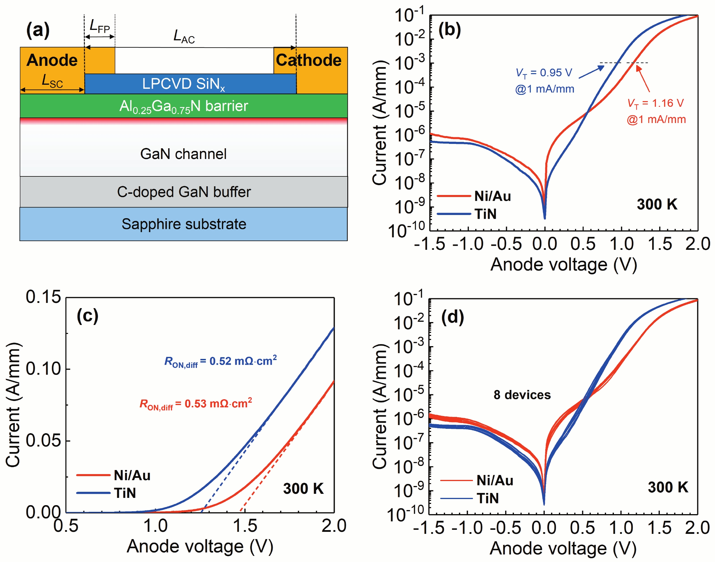
    Fig. 1. (Color online) (a) Schematic cross-section of the fabricated recess-free AlGaN/GaN SBD. IV characteristics of device A and B at RT on the (b) log scale and (c) linear scale. (d) IV characteristics of 8 devices for A and B.
    (Color online) Temperature-dependent I–V characteristics of (a) device A and (b) device B. (c) Dependence of n and qφb on the temperature for both devices. (d) The dependence of qφb on n for two diodes; the extrapolation at n = 1 of the linear fit of the data gives a value of the mean barrier height.
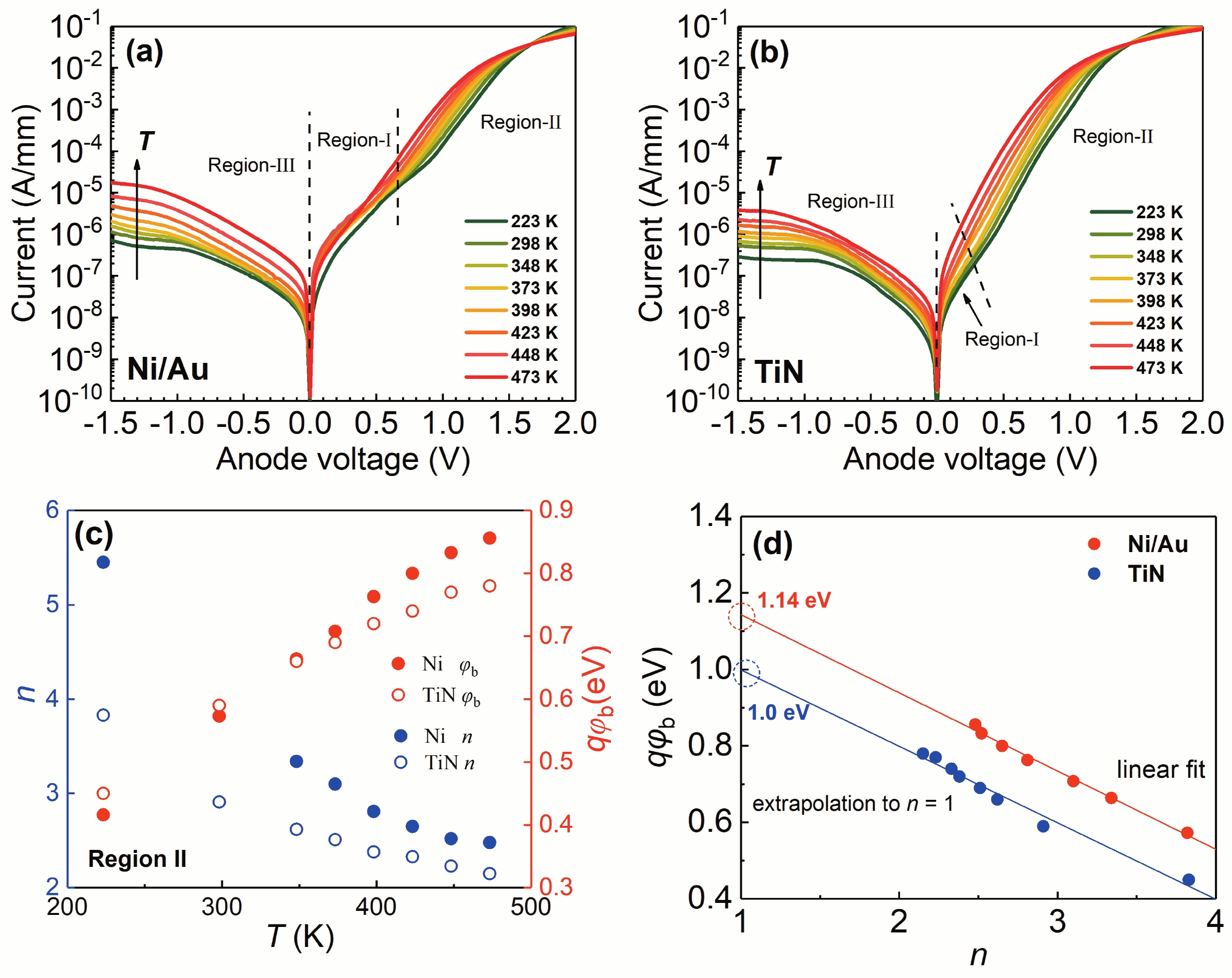
    Fig. 2. (Color online) Temperature-dependent IV characteristics of (a) device A and (b) device B. (c) Dependence of n and b on the temperature for both devices. (d) The dependence of b on n for two diodes; the extrapolation at n = 1 of the linear fit of the data gives a value of the mean barrier height.
    (Color online) (a) Arrhenius plot of IR for both devices. (b) EA extracted from the Arrhenius plot.
    Fig. 3. (Color online) (a) Arrhenius plot of IR for both devices. (b) EA extracted from the Arrhenius plot.
    (Color online) (a) 1 MHz C–V characteristics under the reverse bias voltage. (b) Calculated E–V characteristics under the reverse bias voltage.
    Fig. 4. (Color online) (a) 1 MHz CV characteristics under the reverse bias voltage. (b) Calculated EV characteristics under the reverse bias voltage.
    (Color online) ln(J/E) versus E0.5 at different temperatures for (a) device A and (b) device B. (c) Extracted εs(h) at different temperatures for both devices.
    Fig. 5. (Color online) ln(J/E) versus E0.5 at different temperatures for (a) device A and (b) device B. (c) Extracted εs(h) at different temperatures for both devices.
    (Color online) ln (J/E) versus 1000/T at various temperatures for (a) device A and (b) device B. Extracted qφeff(E) at various temperatures for (c) device A and (d) device B.
    Fig. 6. (Color online) ln (J/E) versus 1000/T at various temperatures for (a) device A and (b) device B. Extracted eff(E) at various temperatures for (c) device A and (d) device B.
    (Color online) ln(J/E2) versus 1/E at low temperature for (a) device A and (b) device B. (c) Extracted qφb from the slope at various temperatures for both devices. (d) Impact of β on qφb extracted by FN model for Ni SBD.
    Fig. 7. (Color online) ln(J/E2) versus 1/E at low temperature for (a) device A and (b) device B. (c) Extracted b from the slope at various temperatures for both devices. (d) Impact of β on b extracted by FN model for Ni SBD.
    (Color online) Schematic band diagram of carrier transport mechanisms at reverse bias for TiN SBD and Ni/Au SBD.
    Fig. 8. (Color online) Schematic band diagram of carrier transport mechanisms at reverse bias for TiN SBD and Ni/Au SBD.
    Hao Wu, Xuanwu Kang, Yingkui Zheng, Ke Wei, Lin Zhang, Xinyu Liu, Guoqi Zhang. Optimization of recess-free AlGaN/GaN Schottky barrier diode by TiN anode and current transport mechanism analysis[J]. Journal of Semiconductors, 2022, 43(6): 062803
    Download Citation