
Hao Wu, Xuanwu Kang, Yingkui Zheng, Ke Wei, Lin Zhang, Xinyu Liu, Guoqi Zhang. Optimization of recess-free AlGaN/GaN Schottky barrier diode by TiN anode and current transport mechanism analysis[J]. Journal of Semiconductors, 2022, 43(6): 062803
- Journal of Semiconductors
- Vol. 43, Issue 6, 062803 (2022)
Abstract
1. Introduction
AlGaN/GaN Schottky barrier diode (SBD) features excellent performance for high-power, high-frequency, and high-temperature applications, attributed to the outstanding properties of GaN material[
The Schottky metal is well recognized to have a considerable impact on the VT and IR of Schottky junction (SJ). For AlGaN/GaN SBD, the most common electrode used as the anode is Ni/Au and TiN metal[
The recess-free technique can improve device uniformity and reliability by eliminating the plasma damage to the AlGaN barrier layer from the etching process[
In this paper, we have achieved the simultaneous improvement of VT and IR for recess-free AlGaN/GaN SBDs by substituting the Ni/Au anode with the TiN anode. The impact of Schottky metal on the electrical properties of SBDs is revealed by analyzing the current transport mechanism.
2. Device structure and fabrication
The epitaxial wafer is a commercial product from the Enkris Semiconductor, grown by MOCVD on a 3-inch sapphire <0001> substrate, consisting of a 1.5 μm C-doped GaN buffer layer, a 400 nm UID GaN channel layer, and a 7 nm Al0.25Ga0.75N barrier layer. With a 24 nm LPCVD-SiNx passivation (780 °C, with RCA pretreatment), the 2DEG channel in the access region was effectively preserved[
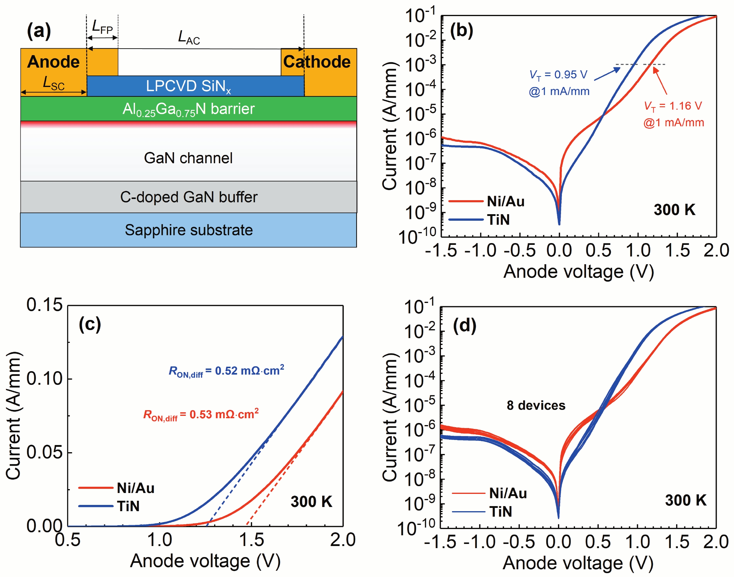
The schematic cross-section of SBD is shown in Fig. 1, and the device fabrication flow is the same except for the anode metal. First, the LPCVD SiNx cap in anode and cathode region was opened with a fluorine-based ICP etch. Then, the metal layer of Ti/Al/Ni/Au (20/150/45/55 nm) was deposited, followed by rapid thermal annealing (RTA) at 870 °C for 50 s in N2 ambient to form the ohmic cathode. Finally, Ni/Au (50 nm/150 nm) was deposited by evaporation to form the anode electrodes for device A, and TiN metal was deposited by reactive sputtering in Ar:N2 (7 : 3 sccm) mixed gas atmosphere to form the anode electrodes for device B. The devices in this work have the same dimensions of LSC/LAC/LFP/W = 2/6/0.75/100 μm. The electrical characteristics of the device were measured with Keysight B1500A.
![]()
Figure 1.(Color online) (a) Schematic cross-section of the fabricated recess-free AlGaN/GaN SBD.
3. Overview of electrical characteristics
The I–V characteristics at room temperature (RT) on the log scale and linear scales are shown in Figs. 1(b) and 1(c), respectively. The SBD with TiN anode exhibits a low VT of 0.94 V (defined as the voltage corresponding to current = 1 mA/mm), a low differential specific on-resistance (RON,diff) of 0.52 mΩ·cm2 and a low IR of ~ 0.5 μA/mm. Compared with SBD with TiN diode, the Ni/Au SBD exhibits similar RON,diff, while presenting a higher VT of 1.16 V and a higher IR of ~1 μA/mm. I–V curves of 8 devices are also plotted in Fig. 1(d), suggesting a good device uniformity attributed to the recess-free technique. The lower VT in TiN SBD can be attributed to the difference between the work function of Ni (~5.15 eV) and of TiN (~4.7 eV)[
4. Current transport mechanisms at forward bias
The I–V characteristics of devices A and B measured from 223 to 473 K are shown in Figs. 2(a) and 2(b) and used to analyze the current transport mechanisms. The I–V characteristics of both devices can be divided into three regions, namely, region-I (low forward bias), region-II (high forward bias), and region-III (reverse bias). In region-I, the current show weak temperature and voltage dependence on the logarithmic axis, indicating that the tunneling-assisted transport mechanism dominates. Obviously, the tunneling effect in this region is more significant for Ni/Au SBD, although the metal work function of Ni is higher than that of TiN. The strong tunneling effect in Ni/Au SBD may be attributed to the interface states existing at the Ni/AlGaN interface caused by the interaction[
![]()
Figure 2.(Color online) Temperature-dependent
where S is the SJ area, A* is the effective Richardson constant of 30 A/(cm·K)2 for Al0.25Ga0.75N[
Fig. 2(c) shows the qφb and n as a function of temperature. It can be observed that both qφb and n show a strong temperature dependence for our devices. This observation is inconsistent with the ideal TE mechanism, in which the qφb and n should be almost constant with temperature. Besides, the calculated values of qφb and n are also far from the ideal value (n = 1, qφb = qφM – χAlGaN), especially at low temperatures. Several studies have suggested that such behavior is attributed to the spatial non-homogeneous distribution of the Schottky barrier height[
5. Current transport mechanisms at reverse bias
In region-III, it can be roughly seen that the temperature dependence of IR varied with temperature for both devices, which indicated IR could be dominated by different transport mechanisms at different ranges of temperature. To identify how many transport mechanisms work, the Arrhenius plots of IR at VA = –0.5 V are drawn in Fig. 3(a). Then, the activation energy (EA) was extracted from the Arrhenius plots, as shown in Fig. 3(b).
![]()
Figure 3.(Color online) (a) Arrhenius plot of
The physical meaning of EA is the energy barrier for electrons at the metal fermi-level to pass through the AlGaN barrier. Therefore, different EA corresponds to different reverse leakage mechanisms. According to the extracted EA in Fig. 3(b), the reverse leakage behavior can be roughly divided into two regions. At high temperatures, as temperature increases, the leakage current shows the apparent temperature dependence, indicating that the thermal emission process could dominate the leakage current in this region. The extracted EA (< 0.6 eV) in this region (Fig. 3(b)) is much smaller than the Schottky barrier height reported in the literature (~ 1 eV)[
Electric field (E) estimation is necessary to analyze IR quantitatively. E across the AlGaN barrier layer can be calculated using the equation E(V) = q[σp– ns(V)]/εsε0[
![]()
Figure 4.(Color online) (a) 1 MHz
5.1. Reverse leakage mechanisms at high temperature
Considering the strong temperature dependence at high temperatures, Poole–Frenkel emission (PFE) is the most probable carrier transport mechanism. The PFE refers to electric-field enhanced thermal emission from a trap state into a continuum of electronic, and the current density of PFE can be described as[
where C is a constant associated with trap concentration, E is the electric field across the barrier, qφt is the barrier height for the electron emission from the trap state, εs(h) = 5.1[
or
From Eq. (4), ln(JPF/E) should be a linear function of E0.5. Figs. 5(a) and 5(b) show that the experimental plots of ln(J/E) versus E0.5 fit well with the linear dependence at different temperatures for both devices, which proves the possibility of PFE. To further confirm the PFE, the εs(h) in Eq. (4) were extracted from the m(T) at different temperatures, as shown in Fig. 5(c). It is found that the εs(h) extracted at high temperature (T > 400 K) is consistent with the theoretical value of Al 0.25Ga0.75N, which strongly indicates that PFE is the dominant mechanism of IR at high temperature. However, at medium and low temperatures (T < 400 K), the extracted εs(h) is much higher than the theoretical value, indicating that different transport mechanisms dominate in this case.
![]()
Figure 5.(Color online) ln(
To identify the defect origin of the trap-involved PFE, the extraction of qφt is necessary. According to Eq. (5), ln(JPF/E) should be a linear function of 1/T, and qφeff(E) can be extracted from the slope. The ln(JPF/E) versus 1000/T plots were shown in Figs. 6(a) and 6(b), it can be seen that the data fit well with straight lines at high temperatures (T > 400 K) with various E. At medium and low temperatures (T < 400 K), the dependence of ln( JPF/E) on temperature is weak, suggesting that the tunneling mechanism dominates in this case, although the data also follows a linear relationship. Then, the extracted E-related qφeff(E) are shown in Figs. 6(c) and 6(d), and the qφt obtained by extrapolating qφeff(E) to zero electric field is 0.65 and 1.02 eV for Ni SBD and TiN SBD, respectively. The value of qφt in Ni SBD and TiN SBD is respectively consistent with the energy level of threading dislocation (TD)[
![]()
Figure 6.(Color online) ln (
The difference in electrically active PFE defects between the two devices can be explained by the N diffusion mechanism based on Fick’s law[
5.2. Reverse leakage mechanisms at low temperature
At low temperatures, the weak temperature dependence of IR indicates that the tunneling process dominates. A possibility is Fowler–Nordheim (FN) tunneling, which is weakly related to temperature but strongly related to barrier height and electric field. The FN current density is given as[
where A = ((q2(m0/m*))/(8πhφb)) is constant, h is Planck’s constant, m0 is the free-electron mass, m* ~ 0.27 is the conduction band effective mass in the barrier layer, estimated by linear interpolation of the values in AlN and GaN[
which indicates that the ln(J/E2) versus 1/E plot should follow a linear dependency if FN tunneling process is the dominating mechanism, and the slope should be a weak function of T. Figs 7(a) and 7(b) show that the calculated ln(J/E2) versus 1/E plot is very consistent with FN tunneling characteristics, indicating that FN tunneling dominates the leakage current at low temperatures for both devices. However, it is found that the qφb of Ni SBD extracted from the slope is much lower than the qφb of TiN SBD (Fig. 7(c)), which is inconsistent with the difference between the work function of Ni (5.15 eV) and TiN (4.7 eV). Moreover, the C–V characteristics (Fig. 4(a)) and the forward I–V characteristics (Figs. 2(c) and 2(d)) show that the qφb of Ni SBD is higher than that of TiN SBD, which is also contradictory to Fig. 7(c).
![]()
Figure 7.(Color online) ln(
It has been found that the ionization of VN donor can cause the thin surface barrier (TSB) effect[
where β is the electric field enhancement coefficient defined as the ratio of the actual electric field to the theoretical electric field. According to Eq. (8), the slope in Figs. 7(a) and 7(b) can be expressed as:
Using Eq. (9), the relationship between β and qφb for Ni SBD can be obtained, as shown in Fig. 7(d).
Fig. 7(d) shows that the extracted qφb increases as β increases. When the β is between 1.5 and 2, the qφb0 for Ni SBD is close to the value reported in the literature[
Curiously, for reverse characteristics, the qφb of TiN is higher than Ni (Fig. 7(c)), while for the forward characteristics, the qφb of TiN is lower than Ni (Fig. 2(d)). This phenomenon can be explained as follows: at high forward bias, the quasi-Fermi level in semiconductor shifts above the level of VN donor, and the ionized VN will be neutralized, so the TSB effect in Ni/AlGaN will be weakened. Besides, the E in AlGaN barrier is decreased with forward bias, and the thermal emission related mechanism will gradually dominate the current transport, so the TSB effect has less influence on the forward characteristics.
In short, the carrier transport mechanisms of both devices are shown by the schematic energy band diagram in Fig. 8. According to the leakage mechanism analysis, it can be concluded that the main reason for the high IR of Ni SBD is that the high-density VN induced by the N diffusion enhances the PFE and FN tunneling. TiN SBD with high N concentrations is efficient to mitigate the N diffusion, thus obtaining a better trade-off between good VT and IR. Therefore, to reduce VN density and improve SBD performance, conductive metal nitride, such as TiN, TaN, and WNx, is more suitable as Schottky metal for AlGaN/GaN SBD.
![]()
Figure 8.(Color online) Schematic band diagram of carrier transport mechanisms at reverse bias for TiN SBD and Ni/Au SBD.
6. Conclusion
In summary, we have comparatively investigated the reverse leakage mechanisms of recess-free AlGaN/GaN SBD with Ni/Au and TiN anodes. It is found that TiN SBD exhibits lower VT and IR than Ni SBD. For forward characteristics, the current of both devices is dominated by the TE mechanism. It is found that both qφb and n show a strong temperature dependence. Such temperature dependence can be explained by the presence of inhomogeneity of the Schottky barrier height, which is proved by the linear relationship between qφb and n. For reverse characteristics, two types of mechanisms work at different temperature ranges. At high temperatures, the IR for Ni/Au anode is dominated by the PFE from VN to the conduction band, while the IR for TiN anode is dominated by the PFE from TD to the conduction band. The decrease of VN can explain the observed low IR in TiN SBD due to the suppression of N diffusion. At low temperatures, the IR of both devices is dominated by FN tunneling. By modifying the FN model, we concluded that the electric field of the barrier layer in the Ni SBD is higher than in the TiN SBD, thus leading to the relatively higher FN leakage in Ni SBD. The TSB effect caused by VN may be responsible for the increased electric field of the barrier layer in Ni SBD.
Acknowledgements
This work was supported in part by Natural Science Foundation of China (Grant No. 61804172), in part by GuangDong Province Key Technologies Research and Development Program (No. 2019B010128001) and in part by the Youth Innovation Promotion Association of CAS.
References
[1] K J Chen, O Häberlen, A Lidow et al. GaN-on-Si power technology: Devices and applications. IEEE Trans Electron Devices, 64, 779(2017).
[2] A Eblabla, X Li, M Alathbah et al. Multi-channel AlGaN/GaN lateral Schottky barrier diodes on low-resistivity silicon for sub-THz integrated circuits applications. IEEE Electron Device Lett, 40, 878(2019).
[3] L Nela, G Kampitsis, J Ma et al. Fast-switching tri-anode Schottky barrier diodes for monolithically integrated GaN-on-Si power circuits. IEEE Electron Device Lett, 41, 99(2020).
[4] M Xiao, Y W Ma, K Cheng et al. 3.3 kV multi-channel AlGaN/GaN Schottky barrier diodes with P-GaN termination. IEEE Electron Device Lett, 41, 1177(2020).
[5] S W Han, J N Song, S H Yoo et al. Experimental demonstration of charge- balanced GaN super-heterojunction Schottky barrier diode capable of 2.8 kV switching. IEEE Electron Device Lett, 41, 1758(2020).
[6] K Dang, J C Zhang, H Zhou et al. Lateral GaN Schottky barrier diode for wireless high-power transfer application with high RF/DC conversion efficiency: From circuit construction and device technologies to system demonstration. IEEE Trans Ind Electron, 67, 6597(2020).
[7] K Dang, J C Zhang, H Zhou et al. A 5.8-GHz high-power and high-efficiency rectifier circuit with lateral GaN Schottky diode for wireless power transfer. IEEE Trans Power Electron, 35, 2247(2020).
[8] S Lenci, B de Jaeger, L Carbonell et al. Au-free AlGaN/GaN power diode on 8-in Si substrate with gated edge termination. IEEE Electron Device Lett, 34, 1035(2013).
[9] J Hu, S Stoffels, S Lenci et al. Performance optimization of Au-free lateral AlGaN/GaN Schottky barrier diode with gated edge termination on 200-mm silicon substrate. IEEE Trans Electron Devices, 63, 997(2016).
[10] J Biscarrat, R Gwoziecki, Y Baines et al. Performance enhancement of CMOS compatible 600V rated AlGaN/GaN Schottky diodes on 200mm silicon wafers. 2018 IEEE 30th International Symposium on Power Semiconductor Devices and ICs, 200(2018).
[11] Y Li, G I Ng, S Arulkumaran et al. AlGaN/GaN high electron mobility transistors on Si with sputtered TiN gate. Phys Status Solidi A, 214, 1600555(2017).
[12] T Kawanago, K Kakushima, Y Kataoka et al. Gate technology contributions to collapse of drain current in AlGaN/GaN Schottky HEMT. IEEE Trans Electron Devices, 61, 785(2014).
[13] L A Li, R Nakamura, Q P Wang et al. Synthesis of titanium nitride for self-aligned gate AlGaN/GaN heterostructure field-effect transistors. Nanoscale Res Lett, 9, 590(2014).
[14] H Kim, M Schuette, H Jung et al. Passivation effects in Ni/AlGaN/GaN Schottky diodes by annealing. Appl Phys Lett, 89, 053516(2006).
[15] H Wu, X W Kang, Y K Zheng et al. Analysis of reverse leakage mechanism in recess-free thin-barrier AlGaN/GaN Schottky barrier diode. Jpn J Appl Phys, 60, 024002(2021).
[16] X W Kang, X H Wang, S Huang et al. Recess-free AlGaN/GaN lateral Schottky barrier controlled Schottky rectifier with low turn-on voltage and high reverse blocking. 2018 IEEE 30th International Symposium on Power Semiconductor Devices and ICs, 280(2018).
[17] X W Kang, Y K Zheng, H Wu et al. Thin-barrier gated-edge termination AlGaN/GaN Schottky barrier diode with low reverse leakage and high turn-on uniformity. Semicond Sci Technol, 36, 094001(2021).
[18] G Sjoblom, J Westlinder, J Olsson. Investigation of the thermal stability of reactively sputter-deposited TiN MOS gate electrodes. IEEE Trans Electron Devices, 52, 2349(2005).
[19] D M Sathaiya, S Karmalkar. Edge effects on gate tunneling current in HEMTs. IEEE Trans Electron Devices, 54, 2614(2007).
[20] S Saadaoui, M Mongi Ben Salem, M Gassoumi et al. Electrical characterization of (Ni/Au)/Al0.25Ga0.75N/GaN/SiC Schottky barrier diode. J Appl Phys, 110, 013701(2011).
[21] A R Arehart, B Moran, J S Speck et al. Effect of threading dislocation density on Ni/n-GaN Schottky diode I-V characteristics. J Appl Phys, 100, 023709(2006).
[22] H Kim, K M Song. Dislocation-related electron transport in Au Schottky junctions on AlGaN/GaN. Trans Electr Electron Mater, 19, 101(2018).
[23] A Chatterjee, S K Khamari, V K Dixit et al. Dislocation-assisted tunnelling of charge carriers across the Schottky barrier on the hydride vapour phase epitaxy grown GaN. J Appl Phys, 118, 175703(2015).
[24] K R Peta, B G Park, S T Lee et al. Analysis of electrical properties and deep level defects in undoped GaN Schottky barrier diode. Thin Solid Films, 534, 603(2013).
[25] R T Tung. Electron transport at metal-semiconductor interfaces: General theory. Phys Rev B, 45, 13509(1992).
[26] R F Schmitsdorf. Explanation of the linear correlation between barrier heights and ideality factors of real metal-semiconductor contacts by laterally nonuniform Schottky barriers. J Vac Sci Technol B, 15, 1221(1997).
[27] D Qiao, L S Yu, S S Lau et al. Dependence of Ni/AlGaN Schottky barrier height on Al mole fraction. J Appl Phys, 87, 801(1999).
[28] D W Yan, H Lu, D S Cao et al. On the reverse gate leakage current of AlGaN/GaN high electron mobility transistors. Appl Phys Lett, 97, 153503(2010).
[29] O Ambacher, J Smart, J R Shealy et al. Two-dimensional electron gases induced by spontaneous and piezoelectric polarization charges in N- and Ga-face AlGaN/GaN heterostructures. J Appl Phys, 85, 3222(1999).
[30] D Mahaveer Sathaiya, S Karmalkar. Thermionic trap-assisted tunneling model and its application to leakage current in nitrided oxides and AlGaN∕GaN high electron mobility transistors. J Appl Phys, 99, 093701(2006).
[31] J R Yeargan, H L Taylor. The Poole-Frenkel effect with compensation present. J Appl Phys, 39, 5600(1968).
[32] H Zhang, E J Miller, E T Yu. Analysis of leakage current mechanisms in Schottky contacts to GaN and Al0.25Ga0.75N∕GaN grown by molecular-beam epitaxy. J Appl Phys, 99, 023703(2006).
[33] Z Q Fang, G C Farlow, B Claflin et al. Effects of electron-irradiation on electrical properties of AlGaN/GaN Schottky barrier diodes. J Appl Phys, 105, 123704(2009).
[34] Z Q Fang, D C Look, D H Kim et al. Traps in AlGaN/GaN/SiC heterostructures studied by deep level transient spectroscopy. Appl Phys Lett, 87, 182115(2005).
[35] T Katsuno, M Kanechika, K Itoh et al. Improvement of current collapse by surface treatment and passivation layer in p-GaN gate GaN high-electron-mobility transistors. Jpn J Appl Phys, 52, 04CF08(2013).
[36] D K Johnstonea, M Ahoujjab, Y K Yeoc et al. Deep centers and their capture barriers in MOCVD-grown GaN. MRS Proc, 692, H2.7.1(2001).
[37] P G Whiting, M R Holzworth, A G Lind et al. Erosion defect formation in Ni-gate AlGaN/GaN high electron mobility transistors. Microelectron Reliab, 70, 32(2017).
[38] A D Koehler, N Nepal, T J Anderson et al. Atomic layer epitaxy AlN for enhanced AlGaN/GaN HEMT passivation. IEEE Electron Device Lett, 34, 1115(2013).
[39] Y N Xu, W Y Ching. Electronic, optical, and structural properties of some wurtzite crystals. Phys Rev B, 48, 4335(1993).
[40] H Hasegawa, T Inagaki, S Ootomo et al. Mechanisms of current collapse and gate leakage currents in AlGaN/GaN heterostructure field effect transistors. J Vac Sci Technol B, 21, 1844(2003).


Set citation alerts for the article
Please enter your email address

© Copyright 2018-2021 | Chinese Laser Press. All Rights Reserved 沪ICP备15018463号-20