
Heyi Huang, Chen Ge, Zhuohui Liu, Hai Zhong, Erjia Guo, Meng He, Can Wang, Guozhen Yang, Kuijuan Jin. Electrolyte-gated transistors for neuromorphic applications[J]. Journal of Semiconductors, 2021, 42(1): 013103
- Journal of Semiconductors
- Vol. 42, Issue 1, 013103 (2021)
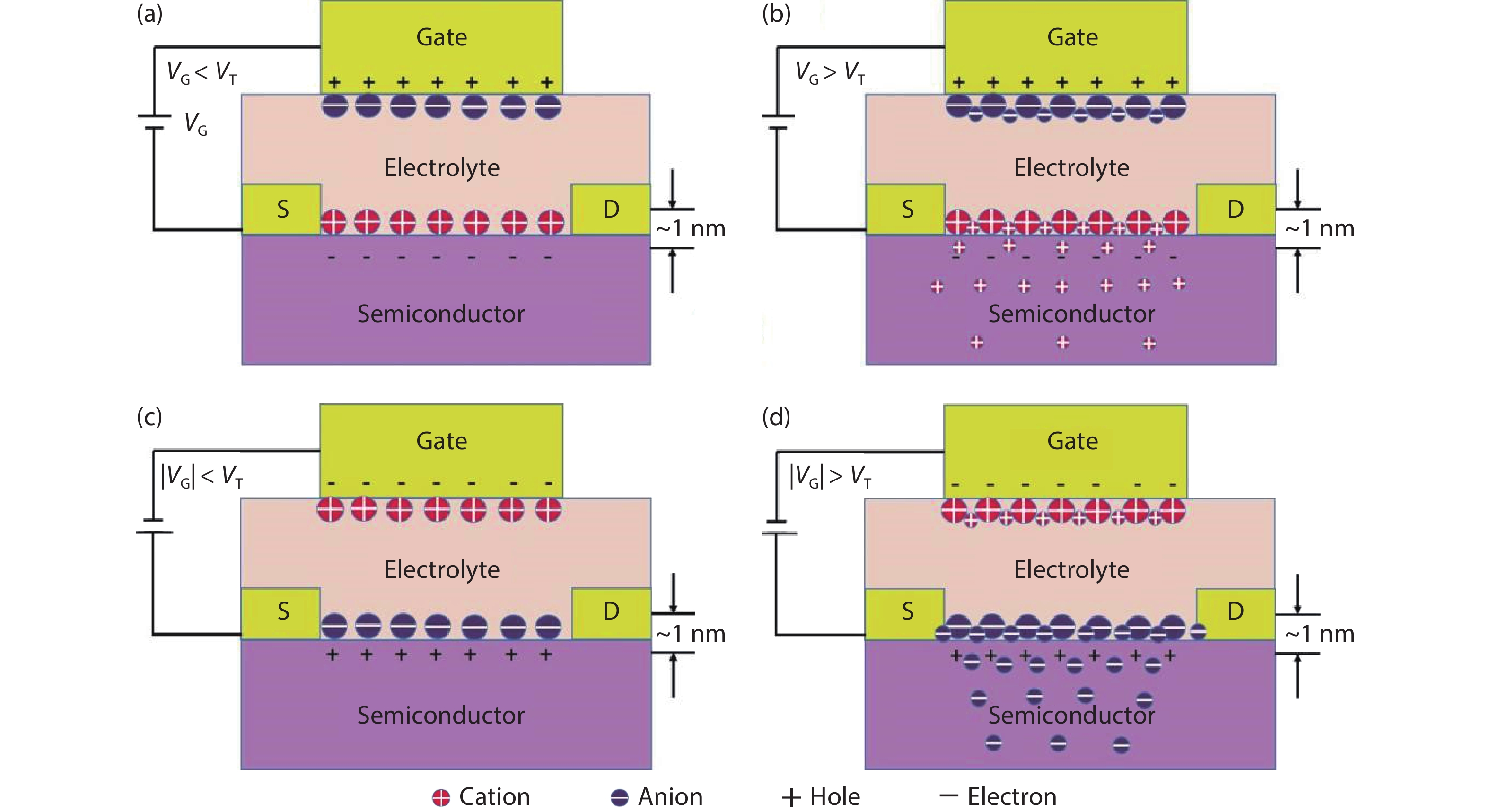
Fig. 1. (Color online) Schematic of the electrolyte-gated transistor operation mechanisms. (a, c) Quasi-static FET operation and (b, d) electrochemical transistors operation. (a) When a positive V G < V T is applied, an EDL is formed at the electrolyte/semiconductor interface (electron doping). (b) When a positive V G > V T is applied, an EDL is formed at the electrolyte/semiconductor interface, but some cations can intercalate into the semiconductor (electrochemical doping). (c) When a negative V G < V T is applied, an EDL is formed at the electrolyte/semiconductor interface (hole doping). (d) When a negative V G > V T is applied, an EDL is formed at the electrolyte/semiconductor interface but some anions can intercalate into the semiconductor (electrochemical doping).
![(Color online) (a) Schematic of a biological synapse[34] and (b) an EGT-based artificial synapse. The synaptic weight (channel conductance) can be modulated in this device using electrochemical intercalation to adjust the small ion concentration in the semiconductor.](/richHtml/jos/2021/42/1/013103/img_2.jpg)
Fig. 2. (Color online) (a) Schematic of a biological synapse[34 ] and (b) an EGT-based artificial synapse. The synaptic weight (channel conductance) can be modulated in this device using electrochemical intercalation to adjust the small ion concentration in the semiconductor.
Fig. 3. (Color online) (a) Evolution of the structural phase via electrolyte gating. (b) Schematic of the SrFeOx transistor design. (c) Sheet conductance versus gate bias. (d) V G-controlled LTP and depression behavior[31 ]. (e) EPSCs stimulated by presynaptic spikes with different amplitudes. (f) Nonvolatile multilevel conductance modulation for SCO devices[32 ].
Fig. 4. (Color online) (a) Schematic of ion dynamics in EGTs. (b) PPF and PTP curves. (c) Three cycles of gating-induced LTP and LTD processes[29 ]. (d) Schematic diagram of hydrogen ion movement during electrolyte gating. (e) Electrolyte-gated VO2 transistor. (f) Synaptic potentiation and depression[33 ]. (g) Schematic structure of a multi-terminal IGZO neuro-transistor[75 ].
Fig. 5. (Color online) (a) A multi-gated architecture of analogous artificial MoS2 synapses[76 ]. (b) Transfer curve. (c) Output characteristics at different top gate biases. (d) EPSC triggered by a series of presynaptic spikes. (e) Energy consumption (left-hand) and the synaptic weight change (right-hand) as a function of pulse amplitudes for one spike[77 ]. (f) Electrochemical graphene synapse[30 ].
Fig. 6. (Color online) (a) Schematic of an organic synaptic transistor using wood-derived cellulose nanopaper (WCN). (b) EPSC values obtained during simultaneous triggering by Gate 1 and Gate 2[39 ]. (c) EPSC signals in response to 10 presynaptic spike trains at different frequencies. (d) Schematic of biological neuronal network and an ONW (organic nanowire) based synaptic transistor. (e) Schematic of EPSC triggered by a pair of spatiotemporally correlated spikes applied to an ONW synaptic transistor via two laterally coupled gates. (f) Postsynaptic current triggered by 60 negative and 60 positive pulses. (g) Array of 144 ONW synaptic transistors fabricated on a 4-inch silicon wafer. Inset: Scanning electron microscopy (SEM) image of a typical ONW with a diameter of 200 nm. (h) Ultraviolet-visible light spectroscopy as a measure of the transparency of bare and ONW array-loaded PET (polyethylene terephthalate) sheets. Inset: Photograph of a bare PET sheet and a 50-mm-pitched ONW array-loaded PET sheet[40 ].
Fig. 7. (Color online) (a) Asymmetric and symmetric STDP functions implemented in ferrite synaptic transistors. (b) Neuromorphic computing simulation[31 ]. (c) Configurable logic operations with dual gating[77 ].
Fig. 8. (Color online) (a) An artificial afferent nerve made of pressure sensors, an organic ring oscillator, and a synaptic transistor[95 ]. (b) Schematic illustration of sound azimuth detection simulation based on the neuro-transistor[64 ]. (c) Classical Pavlov’s dog conditioning experiment[77 ].
|
Table 1. Summary of EGTs on ion species, channel materials, electrolytes, and energy consumption.

Set citation alerts for the article
Please enter your email address
© Copyright 2018-2021 | Chinese Laser Press. All Rights Reserved 沪ICP备15018463号-20