Abstract
Von Neumann computers are currently failing to follow Moore’s law and are limited by the von Neumann bottleneck. To enhance computing performance, neuromorphic computing systems that can simulate the function of the human brain are being developed. Artificial synapses are essential electronic devices for neuromorphic architectures, which have the ability to perform signal processing and storage between neighboring artificial neurons. In recent years, electrolyte-gated transistors (EGTs) have been seen as promising devices in imitating synaptic dynamic plasticity and neuromorphic applications. Among the various electronic devices, EGT-based artificial synapses offer the benefits of good stability, ultra-high linearity and repeated cyclic symmetry, and can be constructed from a variety of materials. They also spatially separate “read” and “write” operations. In this article, we provide a review of the recent progress and major trends in the field of electrolyte-gated transistors for neuromorphic applications. We introduce the operation mechanisms of electric-double-layer and the structure of EGT-based artificial synapses. Then, we review different types of channels and electrolyte materials for EGT-based artificial synapses. Finally, we review the potential applications in biological functions.1. Introduction
Currently, traditional computing is mainly based on the von Neumann architecture, which plays a vital role in many fields. Computers are ideal platforms for solving complex computational problems, such as performing precise numerical calculations. Due to the von Neumann bottleneck, modern computer systems typically use discrete information processing approaches and hierarchical storage, which inevitably limits computational performance efficiency. In addition, traditional computers are confronted by a sharp increase in energy consumption as the speed of calculations has increased. For example, the AlphaGo has 1202 CPUs, 176 GPUs and requires 3000 megajoules for a five-hour match, which is equivalent to 300 days’ energy intake for an adult. These problems become more serious when computers need to handle the tremendous amount of information involving interactions with the real world and imprecisely specified processing.
The human brain is equipped with about 1015 synaptic parallel connection between 1011 neurons, and it can concurrently perform information processing and storage. This has the advantages of faster data processing and lower power consumption (≈ 20 W) over traditional von Neumann computers when performing complex functions such as perception, hearing, vision, motion and so on[1-3]. Hence, the human brain system has attracted scientists around the world to research neuromorphic computing, which is currently manifested in two main approaches: software simulation and hardware implementation. However, software simulation solutions often require huge physical space and a lot of energy consumption. However, these problems can be solved if we apply massively parallel neural networks on hardware.
In hardware, artificial neural networks are constructed using electronic functional devices. The synapse is the basic unit of neuron connection, and it can perform information storage and processing functions through tuning the synaptic weight. In the development of complementary metal–oxide–semiconductor (CMOS)-based digital systems, CMOS analog circuits have been proposed to emulate the synaptic function, but they incur tremendous energy and space costs as complexity increases[3]. Dozens of transistors are required to simulate the function of one synapse. For example, the TrueNorth chip reported by IBM integrated 5.4 billion transistors to implement 1 million neurons and 256 million non-plastic synapses with a newly designed architecture[4]. The inefficiency of simulating the human brain with CMOS-based analog circuits is due to the latter’s digital operation. For example, the energy expenditure of a simple synaptic function, such as excitatory postsynaptic current (EPSC), simulated using CMOS could be extremely higher than the consumption of a biological synapse [4-6].
In recent years, novel electronic/ionic hybrid devices that simulate neuromorphic computing have attracted much attention because they can overcome the shortage of CMOS-based analog circuits[7]. At present, there are two types of these devices. The first type is two-terminal devices[8], including resistive random access memory (ReRAM)[9-12], phase change memory devices (PCM)[13], magnetoresistive random access memory (MRAM)[14-16], ferroelectric tunneling junctions (FTJ)[17-19] and so on. The second type are three-terminal devices[20], including electrolyte-gated transistors[2, 21-23] (EGTs), floating gate transistor devices, and ferroelectric field-effect transistors (FeFETs)[24].
Synaptic devices based on EGTs have attracted considerable attention[25, 26]. In EGTs, the semiconducting channel is in contact with a gate electrode via an ionic conducting and electronic insulating electrolyte. Morphologically, the EGTs devices are the most similar to biological synapses. They provide a good choice for synaptic electronics because of their bionic structure, with physically separated write and read terminals. They can also simulate various neural functions such as short- and long-term plasticity (STP and long-term potentiation (LTP)), spike-timing dependent plasticity (STDP), spatiotemporal information processing, and classical conditioning experiments. Due to their extremely strong electric-double-layer (EDL) effect, synaptic devices based on EDL transistors (EDLTs) usually have very low power consumption. Moreover, the “write” operation of the signals can be carried out in ETGs through gate modulation, while the “read” of the signal is carried out in the channel, which can realize spatial read and write separation. This enables EGTs to integrate information transmission and storage, providing a basis for the realization of more complex neuromorphic computing capabilities.
In this review, the recent research in EGTs for neuromorphic applications is discussed and reviewed. This review is structured as follows. In Section 1, we introduce the mechanisms and types of EGTs. In Section 2, we describe the EGT-based artificial synapse structure. In Section 3, we discuss the channel materials consisting of oxide semiconductors with different active ion types for EGT-based synapses: O2– type EGTs and H+ type EGTs. In Section 4, we review EGT-based synapses with the channel consisting of 2D Materials. Meanwhile, in Section 5, we review EGT-based synapses with the channel consisting of organic semiconductors. In Section 6, we discuss the function of EGTs for neuromorphic computing and biological features imitation. Finally, we provide a conclusion and perspectives for EGTs.
2. Types and mechanisms of EGTs
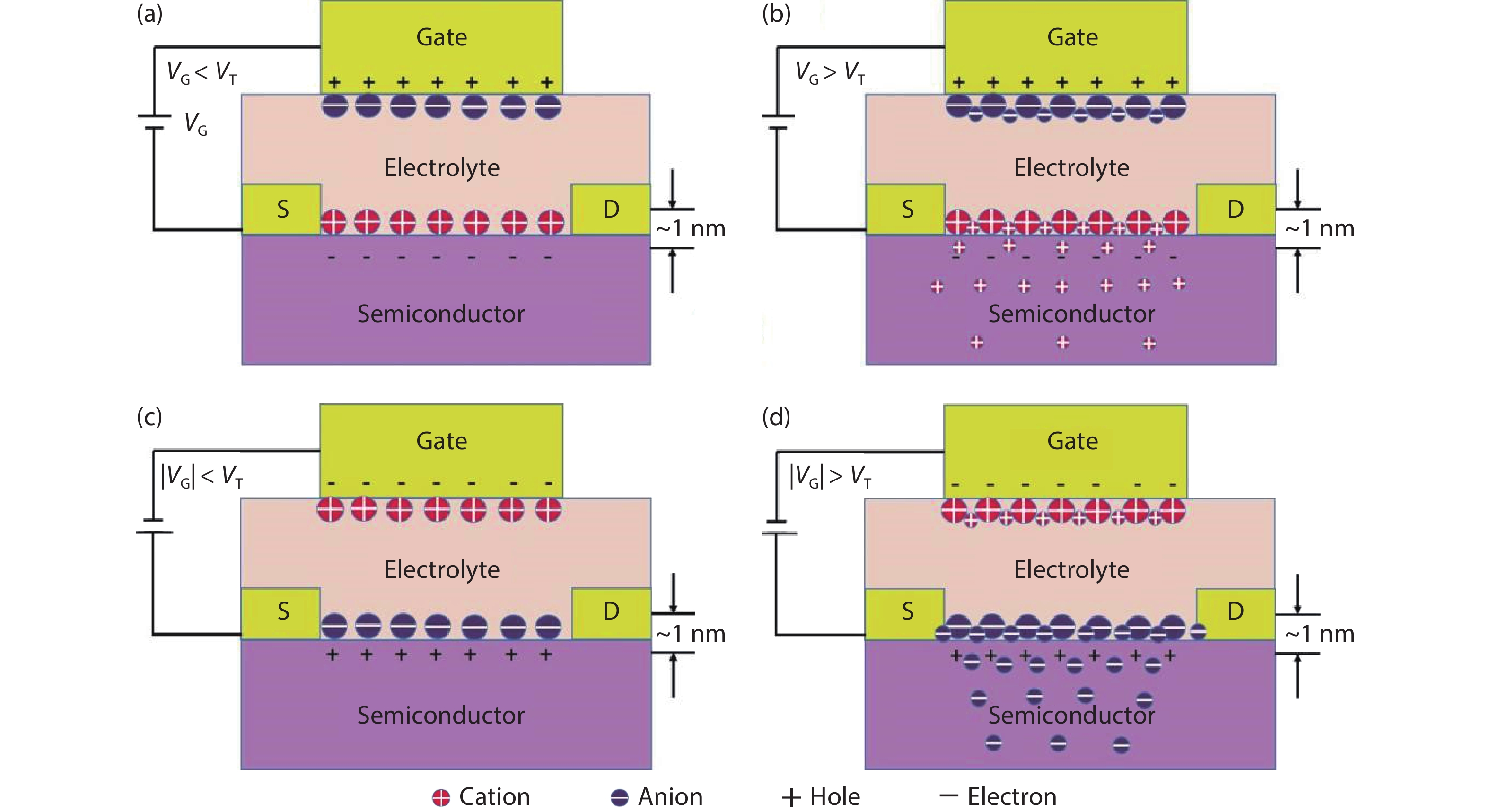
EGTs have two basic operation mechanisms[22], as shown in Fig. 1. The first type is the steady-state (quasi-static) mechanism of EDLTs, as shown in Figs. 1(a) and 1(c). When a voltage (VG) lower than the threshold VT is applied at the gate, this results in migration and accumulation of ions at the gate/electrolyte and semiconductor/electrolyte interfaces. For example, with a positive voltage gate (VG < VT), the anions in the electrolyte migrate toward the interface of gate electrode/electrolyte to compensate the charge build up in the gate electrode. Concurrently, on the other side, the cations in the electrolyte accumulate at the electrolyte/semiconductor interface to form a Helmholtz layer, as shown in Fig. 1(a). The EDLs are only a few nanometers thick. To balance the formation of the EDL at this interface, electrons (or holes) inside the semiconductors accumulate (or deplete) at the solid part of the interface, which can be considered as a nanometer-thick capacitor[27]. Therefore, by varying the applied gate voltage on the electrolytes, the channel resistance can be controlled by the number of charge carriers accumulated at the semiconductor side of the interface[28].

Figure 1.(Color online) Schematic of the electrolyte-gated transistor operation mechanisms. (a, c) Quasi-static FET operation and (b, d) electrochemical transistors operation. (a) When a positive VG < VT is applied, an EDL is formed at the electrolyte/semiconductor interface (electron doping). (b) When a positive VG > VT is applied, an EDL is formed at the electrolyte/semiconductor interface, but some cations can intercalate into the semiconductor (electrochemical doping). (c) When a negative VG < VT is applied, an EDL is formed at the electrolyte/semiconductor interface (hole doping). (d) When a negative VG > VT is applied, an EDL is formed at the electrolyte/semiconductor interface but some anions can intercalate into the semiconductor (electrochemical doping).
In the same way, when a negative voltage gate (|VG| < VT) is applied, the cations in the electrolyte migrate toward the gate electrode/electrolyte interface to compensate the charge build up in the gate electrode. The anions in the electrolyte accumulate concurrently at the electrolyte/semiconductor interface to form a Helmholtz layer, as shown in Fig. 1(c). At steady-state, almost all of the applied gate potential is dropped across the double layers and there is ideally a near zero ionic current from the gate to source electrodes. The few- nanometer- thick EDLs can be considered as nanometer-thick capacitors. The EDL will produce an extremely large electric field. Given that the applied of voltage is lower than the threshold VT, the electric field force is not enough to induce ion insert into the semiconductor material, so the effect of the EDL field mechanism is more like the gating effect in the normal field-effect transistor. Once we remove the gate voltage, the EDLs will disappear after few seconds, which corresponds to a volatile memory of channel modulation.
The second mechanism is based on electrochemical doping. For the ion permeable semiconductor material, when a voltage (VG) higher than the threshold VT is applied at the gate, because of the giant EDL effect, small ions such as H+[29], Li+[30], and O2–[31, 32] can be inserted into the channel and change its doping level, thus controlling the conductance of the channel. As shown in Figs. 1(b) and 1(d), this is a process of electrochemical doping. An electrochemical transistor can realize reversible electrochemical doping and anti-doping (reversible oxidation and reduction reaction) by application of different gate biases. In general, electrochemical doping induces reversible structural changes, such as SrCoOx[32], SrFeOx[31], WO3[29], VO2[33] and so on, which corresponds to the nonvolatile memory of channel modulation.
In this case, a positive VG larger than VT is initially applied; the small cations are accumulated at the semiconductor’s interface forming a strong EDL field and are then injected into the semiconductor, as shown in Fig. 1(b). After applying a negative gate voltage, cations are extracted from the semiconductor channel and de-doping of the semiconductor occurs, resulting in the semiconductor conductance returning to its initial state. Similarly, if a negative VG larger than VT is applied, the small anions are accumulated at the semiconductor’s interface forming a strong EDL field and are then injected into the semiconductors, as shown in Fig. 1(d). After applying a positive gate voltage, anions are extracted from the semiconductor channel and the semiconductor is de-doped.
3. EGT-based artificial synapses
Synapses are the essential units for learning and memory in neural networks. Fig. 2(a) shows a schematic diagram of biological synapses, which consist of three parts: the presynaptic neuron, the synaptic cleft, and the postsynaptic neuron. In biological synapses, information transmission and processing are complex processes. When the synaptic action potential arrives at the presynaptic terminal through the axon, it can trigger the pre-synapse to release to the synaptic cleft a neurotransmitter, such as Ca+, Na+, K+, and Cl–, which is held in the synaptic vesicles before the arrival of the presynaptic action potential. The neurotransmitter diffuses through the synaptic cleft and binds to the receptor proteins on the postsynaptic membrane[1]. Depending on the type of receptor on the postsynaptic membrane, there are two types of synapses: excitatory and inhibitory. The excitatory synapses lead to the excitatory postsynaptic potential/current (EPSP/EPSC) and drive the postsynaptic neuron to generate an action potential. The inhibitory synapses result in the inhibitory postsynaptic potential/current (IPSP/IPSC) and prevent the postsynaptic neuron from generating an action potential. The synaptic weight, which is the connection strength between neurons, can be changed by either or both sides of the synapse. This is referred to as “synaptic plasticity.” The synaptic plasticity can be classified into STP and LTP by the retention time. STP retains only milliseconds to minutes, which consists of the fundamental computational functions in neural networks. LTP retains several hours or longer, which consists of fundamental memory functions in neural network, so that the brain can store a lot of information. Synaptic weights can be simulated by the temporal relationship between presynaptic and postsynaptic spikes, which is called spike-timing-dependent plasticity (STDP)[2].
Figure 2.(Color online) (a) Schematic of a biological synapse[34] and (b) an EGT-based artificial synapse. The synaptic weight (channel conductance) can be modulated in this device using electrochemical intercalation to adjust the small ion concentration in the semiconductor.
In recent years, more and more researchers have exploited the EGTs to simulate synaptic function. Electrolytes are ionic conductors, but they are electronic insulators. The electrolyte can be either liquid or solid, and the ions (anions and cations) in the electrolyte are distributed in the two interfaces with opposite charges under the action of an electric field. EGTs use ions in the electrolyte layer to effectively regulate the electrical conductivity of the device channel.
Thee migration of ions in an electrolyte under the influence of the gate voltage is like the release of neurotransmitters. As shown in Fig. 2(b), similar to biological synapses, the gate electrode of EGTs can be considered to be a presynaptic neuron, the electrolyte is like the synaptic cleft, and the semiconductor channel as a postsynaptic neuron, so the channel conductivity is the equivalent of the synaptic weight. As mentioned earlier, EGTs work in two basic modes: electrostatic modulation and electrochemical doping. When the EGT operates in an electrostatic state, the resulting channel conductance changes can be automatically recovered, providing a basis for modeling STP. When the EGT is in electrochemical doping mode, the channel conductance changes are nonvolatile, which provides the basis for the simulation of LTP, and has nonvolatile and multi-state memory functions. For a biologically synaptic event, the energy consumption is about 10–15 J per pulse. The low energy consumption characteristics of EGTs also allow them to function as ultra-low-energy synaptic devices. Moreover, the “write” operation of signals can be carried out in ETGs through gate modulation, while the “read” of signal transmission lies in the channel’s function; so an EGT can realize spatial read and write separation. This enables EGTs to integrate information transmission and storage at the same time, providing a basis for the realization of more complex neuromorphic functions.
Different channel materials have been investigated in electrolyte-gated synaptic transistors. Moreover, due to the complexity of ion dynamics, ion regulation can be carried out by stimulating the gate with different voltage characteristics, such as pulse width, pulse frequency, and voltage polarity. Channel materials can consist of the following categories: complex metal oxides (e.g., SmNiO3[21], SrCoOx[32], SrFeOx[31], VO2[33]); one-dimensional materials (e.g. carbon nanotube[35, 36]); two-dimensional materials (e.g. graphene[37], TDMs[38]); and organic materials (e.g. cellulose[39], organic carbon nanotubes[40], etc.). The most common classes of electrolytes consist of polymer electrolytes[41-43] [(PEO)/LiClO4[44], (PSSH)[45] and P(VPA-AA)[43]], ionic liquids[46-50] and ionic gels[51-56], inorganic solid-state electrolytes, and so on. From the type of functional ions, the EGTs can be divided into O2–[31, 32], H+[29], Ag+[57], Na+[58, 59] and Li+[60] types. Under a very large electric field, ions can diffuse into the channel material. In the next part we will discuss several ion types for EGTs.
4. Channel materials with oxide semiconductors
4.1. Channel materials with oxide semiconductors: O2−-EGTs
Oxygen ions can be used as functional ions in high-performance electrolyte synaptic transistors[61-63]. In ionic liquid (IL)-gated transistors, the channel can be regarded as a biological postsynaptic neuron and the gate terminal can be regarded as a presynaptic neuron. The water molecules contaminated in ILs can dissociate into H+ and OH– under high gate voltages[29]. Because of the EDL effect, functional ions can be inserted into the channel materials through gating. This process is an electrochemical transistor operation.
The conductivity of some oxides is very sensitive to oxygen content, and several oxides such as SrFeOx (SFO) undergo topotactic phase transition by controlling redox reactions[31]; as shown in Fig. 3(a). In addition, the oxygen content of those oxides can be controlled by using electrolyte gating, which offers many opportunities for designing artificial synaptic transistors. A SFO synaptic transistor is shown in Fig. 3(b). The structure of the channel can be controlled reversibly between the insulating brownmillerite (BM) and conductive perovskite (PV) phases. The transfer curves show a clockwise hysteresis loop in Fig. 3(c). The negative voltage pulses induce the insertion of oxygen ions into the BM-SFO channel, leading to phase transformation from BM-SFO to PV-SFO. In contrast, positive gate pulses can induce the oxygen ion extraction from the channel, thus inducing phase transformation from PV-SFO to BM-SFO. Long-time plasticity is related to memory function in human brain, which consists of LTP and long-term depression (LTD) correspond to strengthening and weakening of synaptic weight. They are still stable after a few minutes to several years. As shown in Fig. 3(d), LTP and LTD behaviors are realized in SFO EGTs by applying 16 consecutive negative pulses (−1.8 V for 5 s, spaced 10 s apart) and 24 consecutive positive pulses (1.8 V for 10 s, spaced 10 s apart). Similarly, the same group designed the EGTs using SrCoOx (SCO)[32]. The EPSCs were induced by presynaptic spikes with different amplitudes in SCO devices, as shown in Fig. 3(e), and the conductance modulation is nonvolatile multilevel (Fig. 3(f)). This process further demonstrated the nonvolatile properties of SCO-based devices.
Figure 3.(Color online) (a) Evolution of the structural phase via electrolyte gating. (b) Schematic of the SrFeOx transistor design. (c) Sheet conductance versus gate bias. (d) VG-controlled LTP and depression behavior[31]. (e) EPSCs stimulated by presynaptic spikes with different amplitudes. (f) Nonvolatile multilevel conductance modulation for SCO devices[32].
Shi et al. demonstrated a liquid electrolyte-gated correlated nickelate (SmNiO3) synaptic transistor with oxygen ions[21]. Applying a negative pulse sequence on the gate electrode increases the conductance of SmNiO3, while applying a positive pulse sequence decreases its conductivity. Owing to this property, asymmetric and symmetric STDP simulations have been achieved.
4.2. Channel materials with oxide semiconductors: H+-EGTs
Protons are the smallest-sized cations that exist in a wide range of solid[64-71] and liquid[72, 73] electrolytes. Due to the low weight and small volume of protons, they can be used as functional ions in electrolyte synaptic transistors. By gating-induced protonation and deprotonation, one can realize reversible phase transformations between various H+ doped phases. Recently, WO3[29] and VO2[33] have been exploited as channel layers for proton-based synaptic transistors.
Yang et al. reported an IL gated EGTs using a WO3 channel, where the absence of A-site cations provides sufficient interstitial space for ion migration[74]. This characteristic makes WO3 an excellent choice for emulating the biological Ca2+ dynamics. A schematic of electrolyte dynamics is shown in Fig. 4(a). Using the quasi-static mechanism and electrochemical H+ doping, they achieved both STP and LTP synaptic functions. STP functions, such as paired-pulse facilitation (PPF) and post-tetanic potentiation (PTP) (Fig. 4(b)), play important roles in decoding temporal information in auditory or visual signals. LTP and LTD (Fig. 4(c)) were simulated by applying a voltage larger than the threshold value of the hydrolysis reaction. The EPSC amplitude gradually increases with positive gate spike, while it decreases to its initial value after negative gate spikes. These results imply that this device can simulate the LTP behavior of synapses. A schematic diagram of protons movement during the electrolyte gating in a VO2 transistor is presented in Fig. 4(d). The VO2 transistor is shown in Fig. 4(e). The single cycle of LTP and LTD process is shown in Fig. 4(f).
Figure 4.(Color online) (a) Schematic of ion dynamics in EGTs. (b) PPF and PTP curves. (c) Three cycles of gating-induced LTP and LTD processes[29]. (d) Schematic diagram of hydrogen ion movement during electrolyte gating. (e) Electrolyte-gated VO2 transistor. (f) Synaptic potentiation and depression[33]. (g) Schematic structure of a multi-terminal IGZO neuro-transistor[75].
Wang et al. reported a neuro-transistor using the proton-conducting solid-state electrolyte, as shown in Fig. 4(g). The device achieved spatiotemporal information processing, imitating the dynamic dendritic discrimination of different spatiotemporal input signals[64].
5. 2D channel materials
Recently, two-dimensional (2D) layered materials[7, 38, 78-81] and quasi-2D transition metal-oxides have shown excellent physical and chemical properties, and thus attracted tremendous interest in imitating artificial synaptic functions. For example, John et al. studied MoS2 neuristors[76], as shown in Fig. 5(a), which are designed to mimic intracellular ion release in chemical synapses using electronic-ionotronic-photoactive approaches. The coexistence of such multiple forms of synaptic plasticity combines memory storage and processing information, enabling efficient novel neuro-network architectures. Fundamental synaptic functions, such as LTP/LTD, STDP, dynamic logic, and classical conditioning behaviors were emulated.
Figure 5.(Color online) (a) A multi-gated architecture of analogous artificial MoS2 synapses[76]. (b) Transfer curve. (c) Output characteristics at different top gate biases. (d) EPSC triggered by a series of presynaptic spikes. (e) Energy consumption (left-hand) and the synaptic weight change (right-hand) as a function of pulse amplitudes for one spike[77]. (f) Electrochemical graphene synapse[30].
Du et al. also fabricated a dual-gated MoS2 transistor[77], which realized synaptic functions and programmable logic operations. In this study, the transfer curve of the MoS2 EGT exhibited an anticlockwise hysteresis, as shown in Fig. 5(b). The device showed a high on/off ratio (≈ 105). The anticlockwise hysteresis behavior by electrolyte gating is ascribed to the EDL and the ion relaxation in the electrolyte. As shown in Fig. 5(c), the output curves exhibited good linearity and good pinch-off characteristics from low to high gate voltages. By using different amplitudes (0.1, 0.5, and 1.5 V) with the same duration time of 5.5 ms to simulate the EPSCs of the synaptic device, we can transform STP to LTP by increasing the presynaptic pulse amplitude; as shown in Fig. 5(d). The energy consumption and the corresponding weight changed following the presynaptic spike amplitude, as shown in Fig. 5(e). The device also showed ultra-low energy consumption of 12.7 fJ in the short-term mode, which is comparable to biological synapses. In addition, they mimic Pavlov’s dog experiment and logic operations such as “And”, “OR”, and “NOT”.
Graphene is another example of a 2D material[30, 37, 82]. Xiong et al. reported an electrochemical graphene synapse[30]. Fig. 5(f) shows the schematic of the graphene synaptic device. The channel conductance of the graphene device is simulated with the synaptic weight. They modulated the synaptic weight by controlling the Li-ions diffusion into graphene layers. The conducting channel consists of graphene, and lithium ion phosphate (LiFePO4 or LFP) was used as the reference electrode. LiClO4 in polyethylene oxide (PEO) was employed as the solid electrolyte. Using this electrochemical approach, the authors achieved reversible and the channel conductance modulation by controlling the Li-ions diffusion. In the electrochemical device, the programming and retention barriers could be decoupled through a circuit switch between the graphene and the solid electrolyte. During the write and read operations, the barrier heights for the memory devices were the same, imposing a balance between the ultra-low programming (write) and retention (read). These graphene synapses displayed long-time retention and endurance performance, energy consumption of ≈ 500 fJ per switching, > 250 distinct states, a symmetrical and linear response.
6. Channel materials with organic semiconductors
Organic semiconductors have many unique characteristics that make them appropriate for use in wearable electronic devices and artificial synapses, such as low fabrication cost[83-87], easy processability, flexibility, low power consumption, easy modification, and biocompatibility[86, 88-95]. Consequently, organic semiconductors have received increasing attention and are now widely considered to be promising candidates for electrolyte gate synaptic transistors[96-102]. Dai et al. reported a synaptic transistor using a C8-BTBT channel that was laterally gated by biodegradable and biocompatible WCN with ionic conductivity[39]. A schematic of the device is shown in Fig. 6(a). The researchers imitated the spatial summation function using C8-BTBT synaptic transistors with two in-plane gates as presynaptic inputs. The EPSC values simultaneously triggered by Gate 1 and Gate 2 are shown in Fig. 6(b). The postsynaptic signal simultaneously triggered by Gate 1 and Gate 2 is larger than that triggered by a single gate (Gate 1 or Gate 2). Therefore, the sub-linear integration was successfully emulated using the C8-BTBT synaptic transistors with dual in-plane gates. The signal filtering characteristics and dendritic integration were simulated in laterally coupled field-effect transistors (LCFETs), as shown in Fig. 6(c). With the increase of presynaptic spike frequency, the EPSC amplitude increased dramatically.
Figure 6.(Color online) (a) Schematic of an organic synaptic transistor using wood-derived cellulose nanopaper (WCN). (b) EPSC values obtained during simultaneous triggering by Gate 1 and Gate 2[39]. (c) EPSC signals in response to 10 presynaptic spike trains at different frequencies. (d) Schematic of biological neuronal network and an ONW (organic nanowire) based synaptic transistor. (e) Schematic of EPSC triggered by a pair of spatiotemporally correlated spikes applied to an ONW synaptic transistor via two laterally coupled gates. (f) Postsynaptic current triggered by 60 negative and 60 positive pulses. (g) Array of 144 ONW synaptic transistors fabricated on a 4-inch silicon wafer. Inset: Scanning electron microscopy (SEM) image of a typical ONW with a diameter of 200 nm. (h) Ultraviolet-visible light spectroscopy as a measure of the transparency of bare and ONW array-loaded PET (polyethylene terephthalate) sheets. Inset: Photograph of a bare PET sheet and a 50-mm-pitched ONW array-loaded PET sheet[40].
Xu et al. designed a synaptic transistor-based on organic nanowires (ONW)[40], as shown in Fig. 6(d), to emulate the functions of a biological synapse. They demonstrated basic spatiotemporal dynamic logic with two laterally coupled gates, as shown in Fig. 6(e). The imitation of LTP and LTD are shown in Fig. 6(f). As shown in Fig. 6(g), 144 large-scale synaptic transistors were fabricated on a 4-inch wafer using highly aligned ONWs. The photograph in Fig. 6(h) showed no obvious reduction in the transparency of PET (polyethylene terephthalate) by the ONW coverage. With a core-sheath-structured ONW active channel and a well-confined 300-nm channel length obtained using ONW lithography, ~1.23 fJ per synaptic event for individual ONW was attained, which rivals that of biological synapses.
7. The function of EGTs for neuromorphic computing and biological features imitation
7.1. EGTs for neuromorphic computing
STDP is essential to emulate a synaptic plasticity mechanism in the neural network[2, 29]. By changing the shape of the preneuron spike waveform, we achieved the asymmetric and symmetric STDP function in SFO EGTs[31] as shown in Fig. 7(a). The SFO EGTs accomplishes the function of handwritten digits recognition as shown in Fig. 7(b). The image recognition accuracy has been calculated using the conductance states in LTP and LTD processes to perform supervised learning with back-propagation of two standard digital, a 8 × 8 pixels of handwritten digits from the “Optical Recognition of Handwritten Digits” dataset (the accuracy approaches 95.2% after 16 training epochs) and 28 × 28 pixels of handwritten digits from Modified National Institute of Standards and Technology (MNIST) dataset (the accuracy approaches 92.7%).
Figure 7.(Color online) (a) Asymmetric and symmetric STDP functions implemented in ferrite synaptic transistors. (b) Neuromorphic computing simulation[31]. (c) Configurable logic operations with dual gating[77].
Logic operations are meaningful to computation performance in a neural network. Du et al. demonstrated that a dual-gated MoS2 transistor can simulate a logic operation such as “AND”, “OR”, and “NOT” operations[77], as shown in Fig. 7(c). Gate 1 (electrolyte gate) and the Gate 2 (back gate) were regarded as two input terminals, while the drain was used for the output terminal. By regulating the conductance state, we can reversibly transform “AND” logic into “OR” logic. We can also manipulate the amplitude of voltage Gate 2 pulses to simulate “NOT” logic.
7.2. EGTs for emulating biological functions
Recently, researchers have made remarkable process in imitating functionalities of the biological nervous system, such as artificial sensory nerves, spatiotemporal information processing, neural emulation, orientation tuning inartificial neurons, the famous classical conditioning of Pavlov’s dog experiments and others. As shown in Fig. 8(a), Kim et al. designed a flexible organic electronics system to simulate an artificial nerve[95]. The artificial afferent nerve consisted of three fundamental components, as shown in Fig. 8(a): (i) pressure sensors, (ii) organic ring oscillators, and (iii) a synaptic transistor. The system simulates the function of a hybrid bioelectronic reflex and consists of two parts: the first uses the multiple tactile receptors to collecting data, the second conveys this information to biological efferent nerves. Multiple tactile receptors are utilized to convert external tactile stimuli into electrical signals. An ion gel-gated synaptic transistor was integrated and converted the electrical signals from multiple ring oscillators into postsynaptic currents. Subsequently, the synaptic transistor could interface with biological efferent nerves to form a complete mono-synaptic reflex arc. To complete a biological reflex arc, the authors connected the artificial afferent nerve to biological efferent nerves of a discoid cockroach and realized the actuation of the tibial extensor muscle in the leg.
Figure 8.(Color online) (a) An artificial afferent nerve made of pressure sensors, an organic ring oscillator, and a synaptic transistor[95]. (b) Schematic illustration of sound azimuth detection simulation based on the neuro-transistor[64]. (c) Classical Pavlov’s dog conditioning experiment[77].
Spatiotemporal information processing is another important function with a high representation density of spatial and temporal information in the human brain. The accurate sound location functionality of the human brain is one of spatiotemporal information processing, which can execute information exchange, avoid danger and other tasks. Wan et al. emulated the function by an oxide-based multi-terminal neuro-transistors[64]. The neuro-transistors showed a large degree of discrimination of different spatiotemporal patterns, emulating the discrimination ability of dendrites for different spatiotemporal patterned stimuli distributed randomly across the dendritic tree. As shown in Fig. 8(b), detecting the interaural time difference (ΔT) in our brain will decide the sound location discrimination. Sound location detection is realized by oxide-based multi-terminal neuro-transistors consisting of dual-gate electrodes (PREN1 and PREN2) and dual-pairs of source/drain terminals (POSTN1 and POSTN2). In the proton-conducting electrolyte-gated transistor, PREN1 and PREN2 are fully linked to POSTN1 and POSTN2, and they are regarded as the left-hand and right-hand ear sound-sensing neurons, respectively. As shown in the neuro-transistors schematic, the connection mode between the PREN1 and POSTN1, and the connection mode between the PREN2 and POSTN2 are straight, while the connection mode between the PREN1 and POSTN2, and the connection mode between the PREN2 and POSTN1 are diagonal, respectively. This indicates that POSTN processes spikes transmitted by the PREN in a weak/strong sequence, while another processes information in the opposite order. The time interval between the two PREN stimuli corresponds to the interaural time difference. The ratio of the amplitude of IPOST2 and IPOST1 at the time of the last PREN signal as a function of the relative timing of the spikes of PREN2 and PREN1 (tPREN2 − tPREN1), and the sound azimuth is shown in Fig. 8(b). The difference between IPOST1 and IPOST2 at the time of the last PREN signal varies with the change of the relative timing of the PREN1 and PREN2 spikes. The relative timing dependent curves of Fig. 8(b) indicates that the simulation of sound location discrimination was achieved.
Pavlov’s dog experiments were conducted to emulate associative learning in the human brain[76, 87]. Du et al. proposed a device that was used to simulate this experiment, as shown in Fig. 8(c), which consisted of a thin-film transistor configuration by using both the Gate 1 (electrolyte gate) and the Gate 2 (the back gate). Gate 1 emulated food/unconditioned stimulus activating salivation/unconditioned response from the postsynaptic terminal, while voltage pulses applied at the Gate 2 emulated bell/conditioned stimulus for the dog activating a conditioned response. The authors performed a six-stage experiment, as follows: (i) feeding the dog simulated the unconditioned stimulus (salivation), that is, the EPSC exceeded the threshold current; (ii) voltage pulses applied at the Gate 2 simulate conditioned stimulus (bell stimulus); (iii) invalid training, the unconditioned stimulus (feeding the dog) and conditioned stimulus (bell stimulus) did not respond by a short time training; (iv) effect train, when the period of time increased to 10 s, the connection between unconditioned stimulus (feeding the dog) and conditioned stimulus (bell stimulus) was strengthened, after which the dog’s salivation could be stimulated by a conditioned stimulus; (v) forgetting, without repeated training with simultaneous unconditioned and conditioned stimulus, the conditioned response would gradually disappear; and (vi) re-conditioning: the connection was restored by applying a shorter time training[77].
8. Conclusion and perspectives
In summary, we provide a review of the recent progress and major trends in the field of EGTs for neuromorphic applications. In the beginning, we introduced two basic operation mechanisms of EDLs: 1) the quasi-static mechanism, and 2) the electrochemical doping mechanism. We introduced the structure of EGT-based artificial synapses and the basis of biological synaptic behavior. We then reviewed different types of channel materials for EGT-based artificial synapses, such as oxide semiconductors (O2−, H+), 2D materials, organic semiconductors, and so on. A comparison among the multiple types of EGTs is shown in Table 1. Finally, imitations of biological functions such as artificial sensory nerves, orientation tuning, and Pavlov’s dog experiments were discussed.
Table Infomation Is Not Enable
Electrolyte-gated synaptic transistors provide novel and clear operating mechanisms for synaptic devices that are proving to be promising techniques for neuromorphic computing. Although they have the advantage of multiple inputs, enabling the device to process data in parallel, perform simultaneous learning, and spatiotemporal dynamic logic function, many challenges still need to be addressed for further practical applications[3, 4], as follows:
1) An increase in the write-read speeds and a reduction in energy consumption are beneficial to the construction of neuromorphic networks. The operation speed of EGTs is mainly limited to kHz. Addressing this requirement pertains to not only selecting channel materials and gate electrolytes with high ion mobility but also understanding what happens at the interface, be it either solid/solid electrolyte or solid/liquid electrolyte. Another technique is to scale down the size of the device, especially by reducing electrolyte thickness to shorten the ion diffusion distance.
2) At present, studies on the array-level computing applications are still in the early stage. To the best of our knowledge, the biggest is a 5 × 6 pixel array with organic synapses, which was demonstrated to mimic the retinal functions[103]. Most recent studies on EGTs are not compatible with standard micro-electronic technology, yet large-scale integration is necessary for neuromorphic computing. Since biological neural networks are arranged in 3D space and require 1015 synaptic connections, the interconnection of EGT synapses is a huge challenge. Therefore, more focus should be directed to improving large-scale integration.
Acknowledgements
This work was supported by the National Key R&D Program of China (No. 2017YFA0303604 and 2019YFA0308500), the Youth Innovation Promotion Association of CAS (No. 2018008), the National Natural Science Foundation of China (Nos. 12074416, 11674385, 11404380, 11721404, and 11874412), and the Key Research Program of Frontier Sciences CAS (No. QYZDJSSW-SLH020).
References
[1] The cell biology of synaptic plasticity. Science, 334, 623(2011).
[2] et alElectric-double-layer transistors for synaptic devices and neuromorphic systems. J Mater Chem C, 6, 5336(2018).
[3] High-performance synaptic transistors for neuromorphic computing. Chin Phys B, 29, 040703(2020).
[4] et alRecent advances in transistor-based artificial synapses. Adv Funct Mater, 29, 1903700(2019).
[5] et alNanoionics-enabled memristive devices: Strategies and materials for neuromorphic applications. Adv Electron Mater, 3, 1600510(2017).
[6] Low-power, adaptive neuromorphic systems: recent progress and future directions. IEEE J Emerg Sel Top Circuits Syst, 8, 6(2018).
[7] Recent progress in synaptic devices based on 2D materials. Adv Intell Syst, 2, 1900167(2020).
[8] et alEnergy-efficient artificial synapses based on oxide tunnel junctions. ACS Appl Mater Interfaces, 11, 43473(2019).
[9] et alStatistical analysis of the impact of anode recess on the electrical characteristics of AlGaN/GaN Schottky diodes with gated edge termination. IEEE Trans Electron Devices, 63, 3451(2016).
[10] et alTraining and operation of an integrated neuromorphic network based on metal-oxide memristors. Nature, 521, 61(2015).
[11] et alNanoscale memristor device as synapse in neuromorphic systems. Nano Lett, 10, 1297(2010).
[12] Memristive crossbar arrays for brain-inspired computing. Nat Mater, 18, 309(2019).
[13] et alStochastic phase-change neurons. Nat Nanotechnol, 11, 693(2016).
[14] A new spin on magnetic memories. Nat Nanotechnol, 10, 187(2015).
[15] et alNeural-like computing with populations of superparamagnetic basis functions. Nat Commun, 9, 1533(2018).
[16] et alTen states of nonvolatile memory through engineering ferromagnetic remanent magnetization. Adv Funct Mater, 29, 1806460(2019).
[17] et alA ferroelectric memristor. Nat Mater, 11, 860(2012).
[18] et alGiant electroresistance in ferroionic tunnel junctions. iScience, 16, 368(2019).
[19] et alReproducible ultrathin ferroelectric domain switching for high-performance neuromorphic computing. Adv Mater, 32, e1905764(2020).
[20] et alRecent progress in three-terminal artificial synapses: From device to system. Small, 15, 1970170(2019).
[21] et alA correlated nickelate synaptic transistor. Nat Commun, 4, 2676(2013).
[22] et alElectrolyte-gated transistors for organic and printed electronics. Adv Mater, 25, 1822(2013).
[23] et alLarge electric field effect in electrolyte-gated manganites. Phys Rev Lett, 102, 136402(2009).
[24] Ferroelectric analog synaptic transistors. Nano Lett, 19, 2044(2019).
[25] et alThe rise of bioinspired ionotronics. Adv Intell Syst, 1, 1900073(2019).
[26] Carbon nanotube synaptic transistor network for pattern recognition. ACS Appl Mater Interfaces, 7, 45, 25479(2015).
[27] et alEndeavor of iontronics: From fundamentals to applications of ion-controlled electronics. Adv Mater, 29, 1607054(2017).
[28] et alHydrogenation-induced surface polarity recognition and proton memory behavior at protic-ionic-liquid/oxide electric-double-layer interfaces. J Am Chem Soc, 132, 6672(2010).
[29] et alArtificial synapses emulated by an electrolyte-gated tungsten-oxide transistor. Adv Mater, 30, 1801548(2018).
[30] et alLow-power, electrochemically tunable graphene synapses for neuromorphic computing. Adv Mater, 30, 1802353(2018).
[31] et alA ferrite synaptic transistor with topotactic transformation. Adv Mater, 31, 1900379(2019).
[32] et alElectrolyte-gated synaptic transistor with oxygen ions. Adv Funct Mater, 29, 1902702(2019).
[33] et alGating-induced reversible HxVO2 phase transformations for neuromorphic computing. Nano Energy, 67, 104268(2020).
[34] Electrolyte-gated transistors for synaptic electronics, neuromorphic computing, and adaptable biointerfacing. Appl Phys Rev, 7, 011307(2020).
[35] A carbon nanotube synapse with dynamic logic and learning. Adv Mater, 25, 1693(2013).
[36] et alPrinted neuromorphic devices based on printed carbon nanotube thin-film transistors. Adv Funct Mater, 27, 1604447(2017).
[37] et alReconfigurable artificial synapses between excitatory and inhibitory modes based on single-gate graphene transistors. Adv Electron Mater, 5, 1902702(2019).
[38] et al2D MoS2 neuromorphic devices for brain-like computational systems. Small, 13, 1700933(2017).
[39] et alWood-derived nanopaper dielectrics for organic synaptic transistors. ACS Appl Mater Interfaces, 10, 39983(2018).
[40] Organic core-sheath nanowire artificial synapses with femtojoule energy consumption. Sci Adv, 2, e1501326(2016).
[41] et alSolution-deposited sodium beta-alumina gate dielectrics for low-voltage and transparent field-effect transistors. Nat Mater, 8, 898(2009).
[42] et alPeriodic array of polyelectrolyte-gated organic transistors from electrospun poly(3-hexylthiophene) nanofibers. Nano Lett, 10, 347(2010).
[43] et alDownscaling of organic field-effect transistors with a polyelectrolyte gate insulator. Adv Mater, 20, 4708(2008).
[44] et alHighly efficient gating and doping of carbon nanotubes with polymer electrolytes. Nano Lett, 4, 927(2004).
[45] et alPolymer field-effect transistor gated via a poly(styrenesulfonic acid) thin film. Appl Phys Lett, 89, 143507(2006).
[46] Potential dependence of the conductivity of highly oxidized polythiophenes, polypyrroles, and polyaniline: finite windows of high conductivity. J Am Chem Soc, 112, 7869(1990).
[47] Solvent-free ionic liquid electrolytes for mesoscopic dye-sensitized solar cells. Adv Funct Mater, 19, 2187(2009).
[48] et alUse of ionic liquids for π-conjugated polymer electrochemical devices. Science, 297, 983(2002).
[49] et alAn efficient organogelator for ionic liquids to prepare stable quasi-solid-state dye-sensitized solar cells. J Mater Chem, 16, 2978(2006).
[50] Materials science. A unique platform for materials design. Science, 321, 50(2008).
[51] et alPrintable ion-gel gate dielectrics for low-voltage polymer thin-film transistors on plastic. Nat Mater, 7, 2291(2008).
[52] et alIon gels prepared by in situ radical polymerization of vinyl monomers in an ionic liquid and their characterization as polymer electrolytes. J Am Chem Soc, 127, 4976(2005).
[53] et alIon gels by self-assembly of a triblock copolymer in an ionic liquid. J Phys Chem B, 111, 4645(2007).
[54] et alIon gel gated polymer thin-film transistors. J Am Chem Soc, 129, 4532(2007).
[55] et alElectrochemical gate-controlled charge transport in graphene in ionic liquid and aqueous solution. J Am Chem Soc, 131, 9908(2009).
[56] et alHigh-density carrier accumulation in zno field-effect transistors gated by electric double layers of ionic liquids. Adv Funct Mater, 19, 1046(2009).
[57] et alIonic/electronic hybrid materials integrated in a synaptic transistor with signal processing and learning functions. Adv Mater, 22, 2448(2010).
[58] et alStructure, sodium ion role, and practical issues for β-alumina as a high-k solution-processed gate layer for transparent and low-voltage electronics. ACS Appl Mater Interfaces, 3, 4254(2011).
[59] A study of vibrational modes in Na+ beta -alumina by molecular dynamics simulation. J Phys: Condens Matter, 6, 1319(1994).
[60] Polymer electrolytes for lithium-ion. Adv Mater, 10, 6(1998).
[61] Metal–insulator transition induced by oxygen vacancies from electrochemical reaction in ionic liquid-gated manganite films. Adv Mater Interfaces, 2, 1500407(2015).
[62] et alPositive colossal magnetoresistance from interface effect in p−n junction of La0.9Sr0.1MnO3 and SrNb0.01Ti0.99O3. Phys Revi B, 71, 184428(2005).
[63] Novel multifunctional properties induced by interface effects in perovskite oxide heterostructures. Adv Mater, 21, 4636(2009).
[64] et alLong-term synaptic plasticity emulated in modified graphene oxide electrolyte gated IZO-based thin-film transistors. ACS Appl Mater Interfaces, 8, 30281(2016).
[65] et alLong-term depression mimicked in an IGZO-based synaptic transistor. IEEE Electron Device Letters, 38, 191(2017).
[66] et alShort-term memory to long-term memory transition mimicked in IZO homojunction synaptic transistors. IEEE Electron Device Lett, 34, 1581(2013).
[67] Inorganic proton conducting electrolyte coupled oxide-based dendritic transistors for synaptic electronics. Nanoscale, 6, 4491(2014).
[68] Chitosan-based biopolysaccharide proton conductors for synaptic transistors on paper substrates. J Mater Chem C, 2, 6249(2014).
[69] Proton-conducting graphene oxide-coupled neuron transistors for brain-inspired cognitive systems. Adv Mater, 28, 3557(2016).
[70] et alMimicking biological synaptic functionality with an indium phosphide synaptic device on silicon for scalable neuromorphic computing. ACS Nano, 12, 1656(2018).
[71] Ionotronic halide perovskite drift-diffusive synapses for low-power neuromorphic computation. Adv Mater, 30, 1805454(2018).
[72] et alDynamically reconfigurable short-term synapse with millivolt stimulus resolution based on organic electrochemical transistors. Adv Mater Technol, 4, 1900471(2019).
[73] et alArtificial synaptic devices based on natural chicken albumen coupled electric-double-layer transistors. Sci Rep, 6, 1(2016).
[74] Electric-field-controlled phase transformation in WO3 thin films through hydrogen evolution. Adv Mater, 29, 1703628(2017).
[75] et alSpatiotemporal information processing emulated by multiterminal neuro-transistor networks. Adv Mater, 31, 1900903(2019).
[76] Synergistic gating of electro-iono-photoactive 2D chalcogenide neuristors: Coexistence of hebbian and homeostatic synaptic metaplasticity. Adv Mater, 30, 1800220(2018).
[77] Dual-gated MoS2 transistors for synaptic and programmable logic functions. Adv Electron Mater, 6, 1901408(2020).
[78] Dual-gated MoS2 neuristor for neuromorphic computing. ACS Appl Mater Interfaces, 11, 41482(2019).
[79] Ion gated synaptic transistors based on 2D van der Waals crystals with tunable diffusive dynamics. Adv Mater, 30, 1800195(2018).
[80] Coplanar multigate MoS2 electric-double-layer transistors for neuromorphic visual recognition. ACS Appl Mater Interfaces, 10, 25943(2018).
[81] et al2D electric-double-layer phototransistor for photoelectronic and spatiotemporal hybrid neuromorphic integration. Nanoscale, 11, 1360(2019).
[82] Graphene dynamic synapse with modulatable plasticity. Nano Lett, 15, 8013(2015).
[83] et alOrganic electronics for neuromorphic computing. Nat Electron, 1, 386(2018).
[84] et alPolymeric electrochemical element for adaptive networks: Pulse mode. J Appl Phys, 104, 114513(2008).
[85] Neurons in polymer: hardware neural units based on polymer memristive devices and polymer transistors. IEEE Trans Electron Devices, 61, 3513(2014).
[86] Frequency driven organic memristive devices for neuromorphic short term and long term plasticity. Org Electron, 65, 434(2019).
[87] Pavlov’s dog associative learning demonstrated on synaptic-like organic transistors. Neur Comput, 25, 549(2013).
[88] et alMulti-gate organic neuron transistors for spatiotemporal information processing. Appl Phys Lett, 110, 083302(2017).
[89] et alNeuroGrid: recording action potentials from the surface of the brain. Nat Neurosci, 18, 310(2014).
[90] et alOrientation selectivity in a multi-gated organic electrochemical transistor. Sci Rep, 6, 27007(2016).
[91] et alIntrinsically ionic conductive cellulose nanopapers applied as all solid dielectrics for low voltage organic transistors. Nat Commun, 9, 1(2018).
[92] Stretchable organic optoelectronic sensorimotor synapse. Sci Adv, 4, 7387(2018).
[93] Spike-timing-dependent plasticity of polyaniline-based memristive element. Microelectron Eng, 185/186, 43(2018).
[94] Neuromorphic functions in PEDOT:PSS organic electrochemical transistors. Adv Mater, 27, 7176(2015).
[95] A bioinspired flexible organic artificial afferent nerve. Science, 360, 998(2018).
[96] Logic gates based on ion transistors. Nat Commun, 3, 1(2012).
[97] et alSynaptic plasticity functions in an organic electrochemical transistor. Appl Phys Lett, 107, 263302(2015).
[98] et alOrientation selectivity with organic photodetectors and an organic electrochemical transistor. AIP Adv, 6, 111307(2016).
[99] Neuromorphic device architectures with global connectivity through electrolyte gating. Nat Commun, 8, 1(2017).
[100] et alA non-volatile organic electrochemical device as a low-voltage artificial synapse for neuromorphic computing. Nat Mater, 16, 414(2017).
[101] et alElectrolyte-gated organic synapse transistor interfaced with neurons. Org Electron, 38, 21(2016).
[102] Artificial synapses based on in-plane gate organic electrochemical transistors. ACS Appl Mater Interfaces, 8, 26169(2016).
[103] et alA Ferroelectric/electrochemical modulated organic synapse for ultraflexible, artificial visual-perception system. Adv Mater, 30, 1803961(2018).