• Photonics Research
  • Vol. 6, Issue 5, 427 (2018)
Eesa Rahimi1、2 and Kürşat Şendur1、*
Author Affiliations
  • 1Faculty of Engineering and Natural Science, Sabanci University, Istanbul 34956, Turkey
  • 2e-mail: eesa@sabanciuniv.edu
  • show less
    DOI: 10.1364/PRJ.6.000427 Cite this Article Set citation alerts
    Eesa Rahimi, Kürşat Şendur. Chimera states in plasmonic nanoresonators[J]. Photonics Research, 2018, 6(5): 427 Copy Citation Text show less
    Simplified model of electron interaction with photons in an active medium with a two-electron, four-energy-level atomic system.
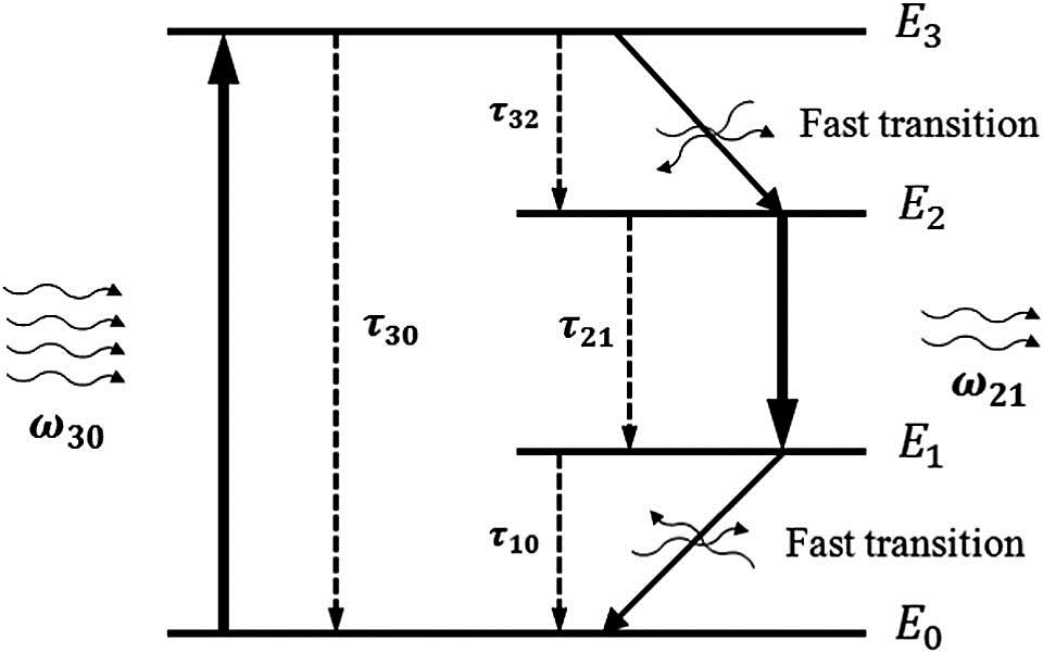
    Fig. 1. Simplified model of electron interaction with photons in an active medium with a two-electron, four-energy-level atomic system.
    Plasmonic nano-oscillator. (a) Geometry and excitation illustration. (b) Electric field enhancement of the plasmonic dimer at the center of its gap with undoped InP. (c) Time profile of the electric field excitation. (d) Probed electric field at the dimer gap with doped InP. (e) Electron population density normalized to the density of active molecules in InP at the center of the plasmonic dimer.
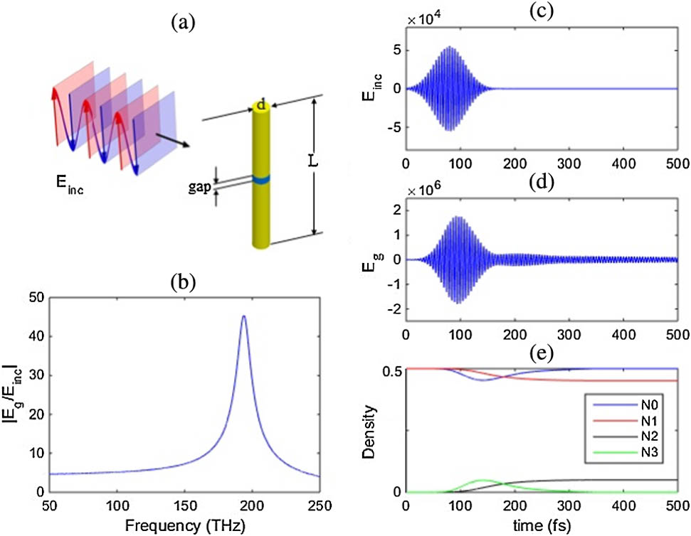
    Fig. 2. Plasmonic nano-oscillator. (a) Geometry and excitation illustration. (b) Electric field enhancement of the plasmonic dimer at the center of its gap with undoped InP. (c) Time profile of the electric field excitation. (d) Probed electric field at the dimer gap with doped InP. (e) Electron population density normalized to the density of active molecules in InP at the center of the plasmonic dimer.
    Array schematic and an example of full coherency in the oscillators. (a) Geometry of the array and the direction of incident plane wave electric field pulse (sketched not to the real scale). (b) Probed electric field at the center of oscillator 1, where the radius of the array r=27.5 nm. Inset shows the electric field at the center of all the oscillators with time. (c) Oscillation amplitude variation for different oscillators over time.
    Fig. 3. Array schematic and an example of full coherency in the oscillators. (a) Geometry of the array and the direction of incident plane wave electric field pulse (sketched not to the real scale). (b) Probed electric field at the center of oscillator 1, where the radius of the array r=27.5  nm. Inset shows the electric field at the center of all the oscillators with time. (c) Oscillation amplitude variation for different oscillators over time.
    Sampled amplitude and phase of oscillator electric fields at their gap for different array geometries with eight oscillators and different disc radii: (a), (b) r=27.5 nm, (c), (d) r=35 nm, (e), (f) r=70 nm, and (g), (h) r=140 nm.
    Fig. 4. Sampled amplitude and phase of oscillator electric fields at their gap for different array geometries with eight oscillators and different disc radii: (a), (b) r=27.5  nm, (c), (d) r=35  nm, (e), (f) r=70  nm, and (g), (h) r=140  nm.
    Sampled phase of oscillator electric fields at their gap for different array geometries with 16 oscillators and different disc radii: (a) r=54 nm, (b) r=68.7 nm, (c) r=137.3 nm, and (d) r=274.6 nm. These radii are selected to keep the inter-oscillator distances the same as those of the corresponding array in Fig. 4.
    Fig. 5. Sampled phase of oscillator electric fields at their gap for different array geometries with 16 oscillators and different disc radii: (a) r=54  nm, (b) r=68.7  nm, (c) r=137.3  nm, and (d) r=274.6  nm. These radii are selected to keep the inter-oscillator distances the same as those of the corresponding array in Fig. 4.
    Eesa Rahimi, Kürşat Şendur. Chimera states in plasmonic nanoresonators[J]. Photonics Research, 2018, 6(5): 427
    Download Citation