
Cizhe Fang, Yan Liu, Qingfang Zhang, Genquan Han, Xi Gao, Yao Shao, Jincheng Zhang, Yue Hao. Germanium-tin alloys: applications for optoelectronics in mid-infrared spectra[J]. Opto-Electronic Advances, 2018, 1(3): 180004
- Opto-Electronic Advances
- Vol. 1, Issue 3, 180004 (2018)
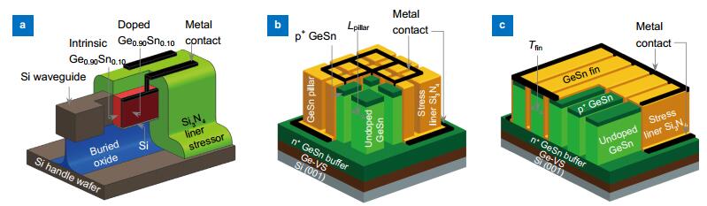
Fig. 1. 3D schematics of the designed GeSn photodetectors based on different architectures.
(a ) GeSn on SOUP waveguide integrated with the Si3N4 liner stressor. Three-dimensional schematics of GeSn detectors with (b ) pillar and (c ) fin array integrated with the Si3N4 liner stressor on Si platform. Figure reproduced from: (a ) ref. 26, Optical Society of America; (b , c ) ref. 33, IEEE.
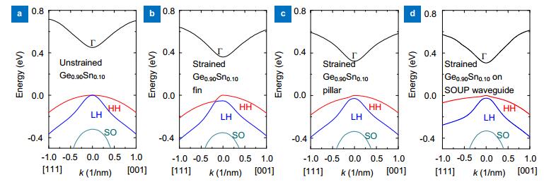
Fig. 2. E-k energy band diagrams of relaxed and strained GeSn devices.
(a ) Relaxed Ge0.90Sn0.10. (b ) Tensile strained Ge0.90Sn0.10 in fin array detector with the L pillar of 200 nm. (c ) Tensile strained Ge0.90Sn0.10 in pillar array detector with the L pillar of 200 nm. (d ) Tensile strained Ge0.90Sn0.10 on SOUP waveguide. Figure reproduced from: (a , b , c ) ref. 33, IEEE; (d) ref. 26, Optical Society of America.
Fig. 3. (a ) Comparisons of the absorption spectra of relaxed and strained GeSn in fin and pillar array detectors at the Sn content of 0.1. L pillar and T fin feature size varys from 100 nm to 500 nm in a step of 100 nm. (b ) Calculated absorption spectra for relaxed and tensile strained GeSn waveguide photodetectors at different Sn content. Figure reproduced from: (a ) ref. 33, IEEE; (b ) ref. 26, Optical Society of America.
Fig. 4. Modeled α as a function of wavelength at different electric fields at (a) Ge0.97Sn0.03, (b) Ge0.95Sn0.05, and (c) Ge0.9Sn0.1, respectively. Figure reproduced from ref. 26, Optical Society of America.
Fig. 5. Mode profiles of both TE and TM modes at different wavelengths in Ge0.90Sn0.10 waveguide. Figure reproduced from ref. 26, Optical Society of America.
Fig. 6. Propagation loss of (a) TE mode and (b) TM mode in tensile strained Ge0.90Sn0.10 waveguide at various biases. Figure reproduced from ref. 26, Optical Society of America.
Fig. 7. 3D schematic of the Ge1-x Snx /Si1-y-z Gey Snz MQW laser wrapped in a Si3N4 liner stressor. Figure reproduced from ref. 36, IEEE.
Fig. 8. Contour plots for (a) ε [100], (b) ε [010], and (c) ε [001] in the normal cross section plane and (d) ε [100], (e) ε [010], and (f) ε [001] in the radial cross section plane in GeSn well for the Ge0.90Sn0.10/Si0.161Ge0.695Sn0.144 MQW laser wrapped in a 500 nm Si3N4 liner stressor. Figure reproduced from ref. 36, IEEE.
Fig. 9. (a ) Modeled J th as a function of the Sn composition in GeSn wells for relaxed and tensile strained GeSn/SiGeSn MQW lasers wrapped in a 500 nm Si3N4 liner stressor. L z is 7 nm and n well is 20. (b ) Modeled optical gain α as a function of injected current density J for the relaxed and tensile strained MQW lasers. Figure reproduced from ref. 36, IEEE.
Fig. 10. 3D schematic of lattice-matched GeSn/SiGeSn DH LED wrapped in a Si3N4 liner stressor. Figure reproduced from ref. 37, Optical Society of America.
Fig. 11. (a ) Modeled strain components as a function of Sn composition in the intrinsic GeSn layer. (b ) Comparison of E G, Γ and E G, L in relaxed and strained GeSn with various Sn compositions. Figure reproduced from ref. 37, Optical Society of America.
Fig. 12. Calculated spontaneous emission spectra for the direct transition of GeSn in the lattice-matched GeSn/SiGeSn DHLEDs (a) under different strain status, (b) with different Sn compositions, (c) with different n injected, and (d) with various n doping. For all the curves, the stronger and weaker peaks represent r sp, HH and r sp, LH, respectively. Figure reproduced from ref. 37, Optical Society of America.
Fig. 13. η IQE versus Sn composition characteristics of lattice-matched GeSn/SiGeSn DH LEDs with the τ SRH of 100 and 50 ns.
(a ) Relaxed and tensile strained GeSn devices. (b ) Strained GeSn devices wrapped in a Si3N4 liner stressor with different values of n injected. (c ) Strained devices with different n doping. Figure reproduced from ref. 37, Optical Society of America.

Set citation alerts for the article
Please enter your email address
© Copyright 2018-2021 | Chinese Laser Press. All Rights Reserved 沪ICP备15018463号-20