1Wide Bandgap Semiconductor Technology Disciplines State Key Laboratory, School of Microelectronics, Xidian University, Xi’an 710071, China
2Key Laboratory for Informatization Electrical Appliances of Henan Province, School of Electric and Information Engineering, Zhengzhou University of Light Industry, Zhengzhou 450002, China
3State Key Laboratory of Power Grid Security and Energy Conservation, China Electric Power Research Institute, Beijing 100192, China
We summarize our work of the optoelectronic devices based on Germanium-tin (GeSn) alloys assisted with the Si3N4 liner stressor in mid-infrared (MIR) domains. The device characteristics are thoroughly analyzed by the strain distribution, band structure, and absorption characteristics. Numerical and analytical methods show that with optimal structural parameters, the device performance can be further improved and the wavelength application range can be extended to 2~5 μm in the mid-infrared spectra. It is demonstrated that this proposed strategy provides an effective technique for the strained-GeSn devices in future optical designs, which will be competitive for the optoelectronics applications in mid-infrared wavelength.
It is known to all that Group Ⅳ semiconductors have been widely applied in electronic devices due to their compatibility with mature complementary metal-oxide- semiconductor (CMOS) technologies and excellent electronic transport properties. However, low luminous efficiency caused by their indirect-bandgap limits their applications in photonic functional devices. Recently, a new technology based on incorporating Sn into Ge has triggered a tremendous interest for the accessibility of the direct bandgap material1-6. The pioneering work has been made by R. Soref and C. H. Perry in ref. 7. After that, subsequent theoretical studies8-11 revealed that an indirect- bandgap material can be tuned to be a direct-bandgap one by increasing the substitutional Sn concentration in the Ge lattice. Moreover, the incorporation of Sn in the Ge lattice not only yields significant red shifts in the band gap energies but also makes it a possible candidate as the gain medium12, 13, which indicates the potential applications of photonics in the mid-infrared (MIR) regions14-17. Up to now, different kinds of efficient devices based on GeSn have been fabricated13, 18, including photodetectors and lasers with a response up to 2 μm.
However, there is a trade-off between high Sn composition and direct bandgap in GeSn based devices due to the fact that solid solubility resulting from high Sn composition would be destructive to the overall function of the optoelectronic device19. Furthermore, the thermal stability of GeSn film caused by high Sn content becomes an obstacle to device fabrication20-24. By inducing a tensile strain into GeSn alloys, the Sn composition can be reduced to achieve direct bandgap compared with the relaxed one2, 25, 26, benefiting their light emission efficiency27, 28. Therefore, silicon nitride (SiNx) films are used as an external stressor to induce tensile or compressive strain into semiconductor29-32, which poses a strategy to improve the optical performance of the strained GeSn-based structures.
We sum up the work of different kinds of optoelectronic devices based on GeSn alloys with the assistance of the Si3N4 liner stressor. Analytical calculations show that the tensile strain induced by Si3N4 liner in GeSn contributes to both device performance and the extension of optical absorption spectrum. It is demonstrated that the proposed strategy could expand the application spectrum of group Ⅳ based devices, which will find important applications in the novel optoelectronic applications.
Device design and characteristic
Photodetector
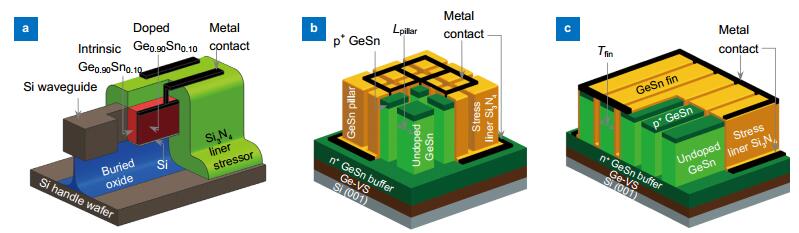
It is worth noting that employing the tensile strained GeSn alloys achieves a material with improved absorption coefficient α in MIR ranging, which provides an effective technique for extending the absorption edge of GeSn to mid-infrared wavelength. Here, we discuss three photodetectors based on different strained GeSn architectures. Figure 1(a) shows a conceptual illustration of the GeSn on Si on oxide undercladding pedestal (SOUP) waveguide. The 3-D schematics of GeSn pillar and fin array detectors are shown in Fig. 1(b) and 1(c), respectively. The tensile strain is introduced in the GeSn material by the Si3N4 liner stressor.
Figure 1.3D schematics of the designed GeSn photodetectors based on different architectures.
(a) GeSn on SOUP waveguide integrated with the Si3N4 liner stressor. Three-dimensional schematics of GeSn detectors with (b) pillar and (c) fin array integrated with the Si3N4 liner stressor on Si platform. Figure reproduced from: (a) ref. 26, Optical Society of America; (b, c) ref. 33, IEEE.
To better analyze the influence of the strain on the energy band, the E-k energy band diagrams of the relaxed and tensile strained Ge0.90Sn0.10 in three different detectors are plotted and compared in Fig. 2. It is observed that in contrast to relaxed GeSn, the EG, Г is obviously reduced in tensile strained GeSn because there is a decline in the energy of Г conduction valleys. It is clear that the EG, Г of tensile strained GeSn in pillar detector exhibits a larger attenuation than that of fin detector. The impacts of geometric parameters on the energy band structure in fin and pillar detectors are discussed in detail in ref. 33. What's more, the impact of Sn content on the E-k energy band for relaxed and tensile strained GeSn is analyzed in ref. 26. It is concluded that by utilizing the Si3N4 liner stressor, the EG, Г of GeSn alloy can be reduced, which is potential to extend the cutoff wavelength of various photonic devices into the MIR region.
Figure 2.E-k energy band diagrams of relaxed and strained GeSn devices.
(a) Relaxed Ge0.90Sn0.10. (b) Tensile strained Ge0.90Sn0.10 in fin array detector with the Lpillar of 200 nm. (c) Tensile strained Ge0.90Sn0.10 in pillar array detector with the Lpillar of 200 nm. (d) Tensile strained Ge0.90Sn0.10 on SOUP waveguide. Figure reproduced from: (a, b, c) ref. 33, IEEE; (d) ref. 26, Optical Society of America.
In order to evaluate the performance of the proposed photodetectors, we calculate the absorption coefficient α, a key parameter for determining the detection spectrum of the detector, by equation (1) 34:
where $\hbar$ is the reduced Plank constant $h/2{\rm{ \mathit{ π} }}$, $\omega $ is the angular frequency, and μ is the reduced mass, which can be calculated by $m_{\rm{e}}^ * m_{\rm{h}}^ * /(m_{\rm{e}}^ * + m_{\rm{h}}^ *)$. The electron and hole effective masses ($m_{\rm{e}}^ * $ and $m_{\rm{h}}^ * $) are extracted from E-k energy band diagrams based on
In equation (2), n is the refractive index, ε0 is the vacuum permittivity, c is the velocity of light, me is the electron mass, and $\Delta $ is the spin-orbit splitting.
Figure 3(a) shows that the calculated absorption coefficient α is modeled as a function of optical wavelength for relaxed and strained Ge0.90Sn0.10 in fin and pillar array detectors with different geometric parameters. It can be clearly seen that the optical response spectra of both strained Ge0.90Sn0.10 fin and pillar detectors are wider than that of relaxed detector. Besides, the pillar detector exhibits a larger cutoff frequency than fin detector when Lpillar and Tfin are equal. With the decrease in fin and pillar dimensions, the cut-off wavelengths display an obvious redshift. It should also be noted that the cut-off wavelengths are extended to be 4.35 μm with the Lpillar of 100 nm. As shown in Fig. 3(b), we investigate the impact of the Sn content on the cut-off wavelengths of both the relaxed and strained devices. A significant redshift of absorption edge can be obtained in the strained devices. Furthermore, the cut-off wavelength performs a greater improvement with a larger Sn composition. All the enhancements in the cut-off wavelength can be speculated that there is an attenuation in the EG, Г of GeSn.
Figure 3.(a) Comparisons of the absorption spectra of relaxed and strained GeSn in fin and pillar array detectors at the Sn content of 0.1. Lpillar and Tfin feature size varys from 100 nm to 500 nm in a step of 100 nm. (b) Calculated absorption spectra for relaxed and tensile strained GeSn waveguide photodetectors at different Sn content. Figure reproduced from: (a) ref. 33, IEEE; (b) ref. 26, Optical Society of America.
In this section, we theoretically investigate tensile strained GeSn electro-absorption modulator based on the Franz-Keldysh (FK) effect. As depicted in Fig. 4, α is modeled as a function of wavelength for tensile strained GeSn waveguide modulators with different Sn content, which is calculated by ref. 26. During simulation, the intensity of electric field varies from 0 to 10 MV/m at a step of 2 MV/m. Although Sn composition is different, the cut-off wavelength of all materials redshifts to MIR spectra range with the increase in the magnitude of electric filed. Furthermore, it is found that the cut-off wavelength increases along with Sn content. To explore the optical transmission properties, here we employ the 2D finite-different time-domain (FDTD) method to model the Ge0.90Sn0.10 waveguide modulator. Mode profiles of transverse electric (TE) and transverse magnetic (TM) modes in the tensile strained Ge0.90Sn0.10 waveguide modulator are plotted at different wavelengths in Fig. 5. The refractive indexes for Ge0.90Sn0.10, Si3N4 and SiO2 are all extracted from ref. 35. Remarkably, single mode transmission can be observed in the waveguide for all the cases. Importantly, there is a leakage of light from waveguide with the increase in wavelength. In order to gain a deeper understanding on the optical transmission characteristics, the propagation loss versus wavelength is calculated for the tensile strained Ge0.90Sn0.10 waveguide under different electric fields in Fig. 6. For both TE and TM modes, it shows a strong dependence of propagation loss on wavelength. The propagation loss increases along with the wavelength since the optical field becomes weakly confined in the waveguide, which corresponds to the mode profiles in Fig. 5. Moreover, for a fixed wavelength, the propagation loss increases with the increase of applied electric field due to the FK effect, which results in an enhancement in the modulation depth of GeSn waveguide electro-absorption modulator.
Figure 4.Modeled α as a function of wavelength at different electric fields at (a) Ge0.97Sn0.03, (b) Ge0.95Sn0.05, and (c) Ge0.9Sn0.1, respectively. Figure reproduced from ref. 26, Optical Society of America.
Figure 5.Mode profiles of both TE and TM modes at different wavelengths in Ge0.90Sn0.10 waveguide. Figure reproduced from ref. 26, Optical Society of America.
Figure 6.Propagation loss of (a) TE mode and (b) TM mode in tensile strained Ge0.90Sn0.10 waveguide at various biases. Figure reproduced from ref. 26, Optical Society of America.
Accessibility of the direct bandgap material makes GeSn a decent alternative to Si in the functional photonic platform, which helps to realize a monolithically integrated laser. A GeSn/SiGeSn multiple quantum well (MQW) laser wrapped in Si3N4 liner stressor is proposed and investigated, as described in Fig. 7. The laser performances are thoroughly analyzed by Sn composition, injected carrier density ninjected, and quantum well number nwell. It is demonstrated that the threshold current density Jth reduces from 476 to 168 A/cm2 and the optical gain is improved obviously, by introducing the Si3N4 liner stressor.
Figure 7.3D schematic of the Ge1-xSnx/Si1-y-zGeySnz MQW laser wrapped in a Si3N4 liner stressor. Figure reproduced from ref. 36, IEEE.
To analyze the impact of the Si3N4 liner stressor on the GeSn/SiGeSn MQW laser, strain distributions on the normal and radial cross section planes are plotted in Fig. 8. The strain along [100], [010], and [001] directions in the normal cross section plane are denoted by ε[100], ε[010], and ε[001], respectively. The strain contour plots indicate that [100] and [010] directions are under a tensile strain while ε[001] is compressive. At the center of the GeSn layer of GeSn/SiGeSn MQW laser, it can be seen that the values of ε[100], ε[010], and ε[001] are 0.85%, 0.85%, and -0.77%, respectively.
Figure 8.Contour plots for (a) ε[100], (b) ε[010], and (c) ε[001] in the normal cross section plane and (d) ε[100], (e) ε[010], and (f) ε[001] in the radial cross section plane in GeSn well for the Ge0.90Sn0.10/Si0.161Ge0.695Sn0.144 MQW laser wrapped in a 500 nm Si3N4 liner stressor. Figure reproduced from ref. 36, IEEE.
As shown in Fig. 9(a) and 9(b), the threshold current density Jth and optical gain α in GeSn/SiGeSn lasers are modeled as a function of Sn composition in GeSn wells and injected current density, respectively. Here, Lz is the thickness of the potential well. By introducing the tensile strain, there is an obvious attenuation in the Jth in Ge0.90Sn0.10/Si0.161Ge0.695Sn0.144 MQW laser. It can be clearly seen that the Jth decreases from 476 to 168 A/cm2 at a Sn content of 0.1. For comparison, the values of ΓMQW, TE·gГ-HH and ΓMQW, TM·gГ-LH are calculated as a function of injected current density J for the relaxed and tensile strained Ge0.90Sn0.10/Si0.161Ge0.695Sn0.144 MQW lasers, as shown in Fig. 9(b). The calculation results indicate that J decreases significantly to achieve a same α for the strained Ge0.90Sn0.10 device. It should also be noted that compared to the Ge0.90Sn0.10/Si0.161Ge0.695Sn0.144 laser, Ge0.96Sn0.04/ Si0.274Ge0.611Sn0.115 device performs an improved J under the same tensile strain, indicating the influence of the Sn component.
Figure 9.(a) Modeled Jth as a function of the Sn composition in GeSn wells for relaxed and tensile strained GeSn/SiGeSn MQW lasers wrapped in a 500 nm Si3N4 liner stressor. Lz is 7 nm and nwell is 20. (b) Modeled optical gain α as a function of injected current density J for the relaxed and tensile strained MQW lasers. Figure reproduced from ref. 36, IEEE.
To better understand the impact of the gain medium on photoluminescence inside the cavity, a brief introduction is presented from the energy band structure. The subband energy difference between EΓ and EL is defined as ΔE. Here, EΓ and EL are the energies of the ground sub-band levels of Γ and L valleys, respectively. Large density of the states concentrates in L-bandedge due to the fact that the effective mass is large. It is recognized that injected carriers occupy firstly lower energy states. Consequently, there is a larger carrier leakage for large ΔE and a small value of ΔE of the material is preferable to increase the gain. Energy band structure and carrier distribution in GeSn/SiGeSn MQW are discussed in detail in ref. 36. According to the discussion above, under tensile strain, the band structure is changed. During the injection of carriers, the population inversion between the sub-bandgap Esub-G in GeSn wells occurs for the increase of electron occupation probability in Γ conduction valley, which contributes to the improvement of light emission performance in lasers. It is believed that the Sn compositions at well layers and the strain should be carefully designed to achieve a large optical gain.
Light-emitting diode
In consideration of few experimental studies on the tensile strained GeSn light emitters up to date, we theoretically design and analyze a GeSn/SiGeSn double heterostructure (DH) light emitting diode (LED) with a microdisk structure wrapped in Si3N4. The impacts of Sn content on strain distributions and energy band structure are thoroughly analyzed. Moreover, the analysis of simulation results shows that the spontaneous emission rate rsp and the internal quantum efficiency ηIQE can be improved by increasing Sn composition, carrier injection density ninjected, and n-type doping concentration ndoping in the GeSn active layer. The 3D schematic of a GeSn/SiGeSn DH LED with a microdisk device architecture is shown in Fig. 10.
Figure 10.3D schematic of lattice-matched GeSn/SiGeSn DH LED wrapped in a Si3N4 liner stressor. Figure reproduced from ref. 37, Optical Society of America.
The values of ε[100],
ε[010], and ε[001], and volume strains in the central region for intrinsic GeSn layers are determined by the finite element method (FEM), which are extracted and compared in Fig. 11(a). One can see that there is no more change in the strain distribution. Figure 11(b) gives the EG, Γ and EG, L of the relaxed and strained GeSn with different Sn compositions. It can be observed that under the tensile strain, the energy of the Γ conduction valley and L conduction valley declines with the increase in Sn content. It should also be noted that the energy of the Γ conduction valley decreases more significantly than that of the L conduction valley, which leads to a decline of Sn content required for achieving the direct bandgap.
Figure 11.(a) Modeled strain components as a function of Sn composition in the intrinsic GeSn layer. (b) Comparison of EG, Γ and EG, L in relaxed and strained GeSn with various Sn compositions. Figure reproduced from ref. 37, Optical Society of America.
Since the light-emitting performance of the devices is dependent on rsp and ηIQE, we first focus on rsp. Detailed calculation of rsp per unit volume in the energy and ηIQE can be seen in the ref. 37. As depicted in Fig. 12, the total spontaneous emission spectra of the proposed device are plotted under different conditions. Considering that there are two valence bands (e.g. a light hole (LH) band and a heavy hole (HH) band), rsp, LH and rsp, HH are calculated, respectively, corresponding to two peaks in the spontaneous emission spectrum. Compared to the relaxed one, rsp can be improved markedly in the strained device. Figure 12(b) compares the total spontaneous emission spectra with different Sn compositions. It can be clearly seen that with the same ninjected, the spontaneous emission spectra of the strained GeSn increase with the Sn content. With the same doping condition, a rapid increase in the intensity can be observed in Fig. 12(c), suggesting the similar impact of Sn content and ninjected on the strength of spontaneous emission rate. Besides, it is worth noting that the increases of Sn composition and ninjected bring about an opposite shift of peak position. That is, the redshift is caused by increasing Sn composition while the blueshift results from improved ninjected. Figure 12(d) describes the impact of ndoping on rsp, which shows that rsp can exhibit an enhancement with the increase in the n-type doping concentration ndoping.
Figure 12.Calculated spontaneous emission spectra for the direct transition of GeSn in the lattice-matched GeSn/SiGeSn DHLEDs (a) under different strain status, (b) with different Sn compositions, (c) with different ninjected, and (d) with various ndoping. For all the curves, the stronger and weaker peaks represent rsp, HH and rsp, LH, respectively. Figure reproduced from ref. 37, Optical Society of America.
As another key factor to evaluate the light-emitting performance of the devices, the ηIQE is calculated as a function of Sn composition in Fig. 13. The defect-limited carrier lifetime is denoted by τSRH, which can be increased by improving the material quality of GeSn. It seems that ηIQE can be improved along with Sn content in GeSn layer and the devices with a large τSRH achieve an enhancement in ηIQE compared to those with a small τSRH. It can be seen from Fig. 13(a) that ηIQE of DH LEDs is enhanced significantly after introducing tensile strain for the increase of ne, Γ/ne, total in the tensile strained GeSn. Here, the total electron concentration ne, total is the sum of those in Γ and L valleys (ne, Γ+ne, L). The impacts of ninjected and ndoping on ηIQE are investigated and shown in Fig. 13(b) and 13(c). It seems that ηIQE shows similar ninjected-depengence and ndoping-dependence like rsp. That is, the increase of ninjected and ndoping can also improve ηIQE of the devices.
Figure 13.ηIQE versus Sn composition characteristics of lattice-matched GeSn/SiGeSn DH LEDs with the τSRH of 100 and 50 ns.
(a) Relaxed and tensile strained GeSn devices. (b) Strained GeSn devices wrapped in a Si3N4 liner stressor with different values of ninjected. (c) Strained devices with different ndoping. Figure reproduced from ref. 37, Optical Society of America.
In the last part of this section, we will briefly discuss the possible future avenues in GeSn material. Considering that band gap can be adjusted by adding Sn content, GeSn material can be applied for light emitting devices, including laser and LED. It has been reported that the related work is underway in laser38-40 and light emission41-43. However, most of work is just focused on optical pumping at low temperature and the luminous efficiency is low. GeSn material with direct bandgap leads to a small band gap (i.e., ~0.56 eV), which limits its applications in optical communication44. Besides, the existence of solid solubility and limitation of strain engineering also influence the performance of GeSn based devices. Above all, the photodetector with GeSn is potential for the feasibility of practical applications. It is demonstrated that there are already some achievements in photodetection45-46. Due to the tremendous research attention to this material, the growth of GeSn film is correspondingly explored to improve the stability and quality of GeSn film for the development of GeSn-based photonic applications47-49. Owing to the fast growing rate of the research on this material, the author is confident that more breakthroughs in practical applications will be achieved.
Conclusion
In summary, we discuss the recent achievements in the applications of GeSn based devices wrapped by the Si3N4 liner stressor. Their strain distribution is analyzed in detail by numerical simulation tools, which is introduced by the Si3N4 liner stressor. The calculations show that the performance can be improved by optimizing the geometric parameters. Importantly, the operating wavelength can be extended to the whole mid-infrared (2~5 μm) region, which paves the way for the monolithic and CMOS- compatible mid-infrared integrated optics applications like image sensors and optical receivers.
Acknowledgements
The authors thank National Natural Science Foundation of China (Grant No. 61534004, 61604112 and 61622405).
Competing interests
The authors declare no competing financial interests.
[34] P K Basu. Theory of Optical Processes in Semiconductors: Bulk and Microstructures (Oxford, UK: Clarendon, 1997)..
[35] E D Palik. Handbook of Optical Constants of Solids (San Diego: Academic, 1998)..
[36] Y Liu, C Z Fang, X Gao, G Q Han, Q F Zhang et al. Theoretical investigation of tensile-strained GeSn/SiGeSn multiple quantum well laser wrapped in Si3N4 liner stressor. IEEE Photonics J, 10, 1500609(2018).
[45] C H Tsai, G E Chang. GeSn/Ge quantum well photodetectors for short-wave infrared photodetection: experiments and modeling. Proc SPIE 10231, 10231, 102310J(1023).
[47] P C Grant, W Dou, B Alharthi, J M Grant, A Mosleh et al. Comparison study of the low temperature growth of dilute GeSn and Ge. Jf Vac Sci Technol B Nanotechnol Microelectron Mater Process Meas Phenom, 35, 061204(2017).