Mohammad Hosseini, Hassan Kaatuzian, Iman Taghavi. Graded index separate confinement heterostructure transistor laser: analysis of various confinement structures[J]. Chinese Optics Letters, 2017, 15(6): 062501
Copy Citation Text
A new configuration of the confinement structure is utilized to improve optoelectronic performance, including threshold current, ac current gain, optical bandwidth, and optical output power of a single quantum well transistor laser. Considering the drift component in addition to the diffusion term in electron current density, a new continuity equation is developed to analyze the proposed structures. Physical parameters, including electron mobility, recombination lifetime, optical confinement factor, electron capture time, and photon lifetime, are calculated for new structures. Based on solving the continuity equation in separate confinement heterostructures, the threshold current reduces 67%, the optical output power increases 37%, and the 3 dB optical bandwidth increases to 21 GHz (compared to 19.5 GHz in the original structure) when the graded index layers of ( in the left side of quantum well, in the right side of quantum well) are used instead of uniform GaAs in the base region.
Carrier transport across the separate confinement heterostructure (SCH) has substantial effects on dc and ac characteristics of quantum well (QW) lasers[1]. Also, the carrier population of QW excited states, which depends on the confinement structure, plays an important role in the threshold specifications of SCH and graded index (GRIN) SCH QW lasers[2]. The heterojunction bipolar transistor laser (HBTL) is a type of QW laser, containing one (or a few) QW(s) and two SCHs in its base region, where the carrier dynamics are governed by various structural factors. The transistor laser (TL) that we study here is based on an npn heterojunction bipolar transistor (HBT) (n-InGaP/p-GaAs/n-GaAs) with an emitter area of [3]. In GaAs-based HBTs, the common approach to establish a quasi-electric field is linearly grading the aluminum (or indium) content of AlGaAs (or InGaAs)[4]. In this Letter, we employ GRIN layers of instead of simply uniform GaAs in the base region to achieve various levels of confinement.
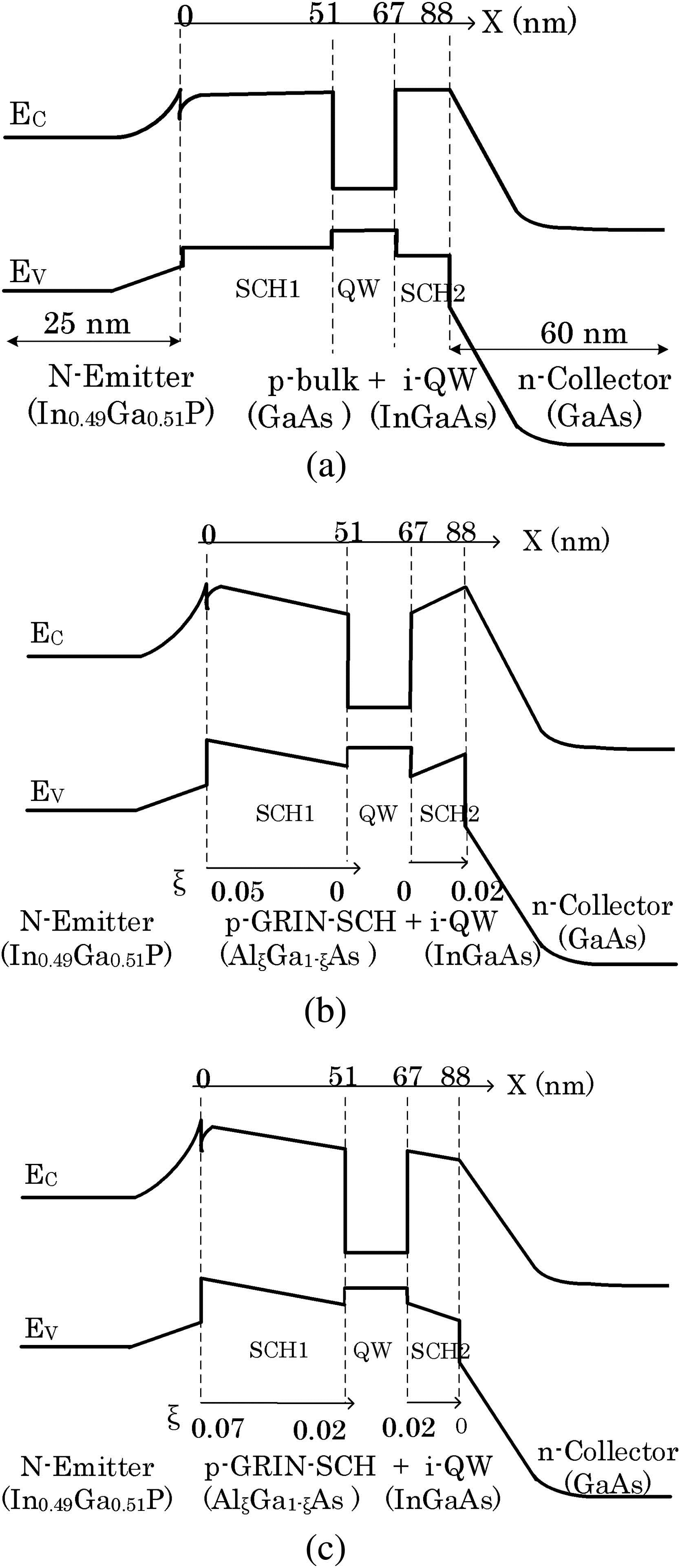
The energy band diagram of the primary TL proposed by Feng and Holonyak[3] under forward bias is depicted in Fig. 1(a), named the first structure in this Letter. In the first proposed design, called the second structure, the GRIN layers of are used [Fig. 1(b)]. In the third structure, GRIN layers of are used [Fig. 1(c)]. Calculating the slope of the conduction band profile, we gain an estimate for the induced built-in potential in SCH1 and SCH2. The energy gap of the material (in eV) at is determined by ,. The induced built-in potential can be achieved using , where is the SCH width, and denotes the bandgap energy difference at two sides of the SCH regions, resulting in a magnitude of and for the induced built-in potential of SCH1 and SCH2, respectively. These values of quasi-electric fields are in good agreement with the experimental values reported in Refs. [4,5].
Figure 1.Schematic energy band diagram of (a) the primary TL proposed by Feng and Holonyak[3] (first structure), (b) first proposed GRIN-SCH structure, (second structure), and (c) second proposed GRIN-SCH structure (third structure) under forward bias. Slope of the band diagram in SCH1 and SCH2, which determines the magnitude of the quasi-electric field.
To analyze the proposed structures, the equation for the electron current density, including both drift and diffusion components, can be written as where is the base electron concentration, and is the diffusion constant. The continuity equation describing the injected minority electron population transporting from the emitter to the collector is where is the base recombination lifetime. Combining Eqs. (1) and (2), the following equations for the SCH1 and SCH2 regions can be obtained under the steady-state condition (): where and are the effective minority electron mobilities, corresponding to SCH1 and SCH2, and and are the average recombination lifetimes related to SCH1 and SCH2, respectively. The boundary conditions needed to solve Eqs. (3) and (4) are , and , where is the carrier density of the virtual states (VS) located at . The current density of the VS (), including both the drift and diffusion components, is
Sign up for Chinese Optics Letters TOC. Get the latest issue of Chinese Optics Letters delivered right to you!Sign up now
Finally, the emitter and collector current densities are found by
Also, the current relation of the transistor is .
The laser is described by the conventional laser rate equations[6]
The QW in the base location adds another recombination region that has a variable recombination rate; spontaneous emission below the laser threshold and stimulated emission above the laser threshold. Carriers at are located at the virtual bound states. The carriers entering the VSs have two possibilities, falling in the QW states or diffusing to the collector. Equations (11) and (12) make appropriate connections between carrier densities and current densities related to the QW (, ) and VS[7]:
In the above equations, is the photon density, is the optical confinement factor, denotes the optical gain, is the gain compression factor, is the spontaneous emission, is the QW width, is the spontaneous emission lifetime, and is the escape lifetime from the QW to the VS[8]. is the overall capture lifetime for the QW[9].
The semiconductor optical gain function is defined as where is the transparency electron density, is the dc value of photon concentration, and is the differential gain of the active layer. Our focus in this Letter is to apparently not alter the active region (i.e., the QW), but the SCH. The QW parameters, including and , were left unchanged in our study. In our previously published Letter, considering ground, first and second excited states, strain effects, and the calculation of quasi-Fermi levels of the conduction and valence band, a nonlinear carrier-dependent gain of the TL is developed, from which we extracted the gain parameters, i.e., and , as a function of device structural factors[10].
The threshold gain () for all three structures is calculated using the optical confinement factor () and optical loss () of each structure, where is the laser cavity length, and and are the facet reflectivity.
Around the threshold point, , and . Using Eq. (10), it can be shown that
From the calculated value of , we deduce the corresponding , which gives the value of current density at transparency via the relation . The threshold current density is obtained using , where denotes the QW lattice constant, and is the internal quantum efficiency[11].
Minority electron mobility in highly doped was calculated in Ref. [12], while other physical parameters of the multiple QW (MQW) TL, including the diffusion constant, carrier lifetimes, and optical confinement factor, are calculated by Taghavi et al.[9]. All of the physical parameters for the new proposed structures are calculated and summarized in Table 1.
Structure
Device Parameter
Symbol
Unit
Calculation Approach Ref.
1st
2nd
3rd
Effective minority electron mobility
SCH1
μ1
cm2/Vs
[12]
1068
964.7
919.325
SCH2
μ2
cm2/Vs
1068
1014.05
1014.05
Diffusion constant
SCH1
D1
cm2/s
[4]
27.61
24.88
23.71
SCH2
D2
cm2/s
27.61
26.16
26.16
Quasi-electric field
SCH1
ε1
V/cm
[4]
0
1.22×10⁴
1.22×10⁴
SCH2
ε2
V/cm
0
1.18×10⁴
1.18×10⁴
Effective recombination lifetime
SCH1
τB1
ps
[9]
201
220
243
SCH2
τB2
ps
201
210
210
Optical confinement factor
Γ
%
[9]
5.82
5.65
5.51
Optical loss
αi
cm−1
[9]
20.14
19.56
19.07
Photon lifetime
τp
ps
[9]
2.57
2.59
2.61
Electron capture time
τcap
ps
[9]
0.90
0.56
0.57
Table 1. Calculated Physical Parameters for All Three Structures
Solving Eqs. (3) and (4) for increasing the base current, the minority electron density in the base region can be calculated as shown in Fig. (2). Compared with the calculated electron distribution for the standard single QW (SQW) TL in Refs. [3,13], the excited electron population in the QW position is the maximum in the first proposed design [Fig. 2(a)]. Figure 2(a) is in good agreement with the calculated carrier population in the barrier layer for the linear GRIN-SCH QW laser discussed in Ref. [14]. Figure 2(b) also complies with the results of the graded base HBTs discussed in Ref. [4].
Figure 2.Calculated minority electron distribution for (a) the first proposed GRIN-SCH structure and (b) the second proposed GRIN-SCH structure. (a) is in good agreement with the calculated carrier population for the GRIN-SCH QW laser[14], and (b) also complies with the results of graded base HBTs[4].
Considering the drift component, moreover the diffusion term, the collector current density can be achieved using Eq. (7). Figure 3 shows the variation of the dc current gain () for all three structures. The dc current gain reduces significantly when second structure is employed. As shown in Fig. 2(a), the number of captured electrons in the QW position is the maximum value; as a result, the proportion of electrons captured by the collector is smaller, and, therefore, we should expect a reduction in the current gain.
Figure 3.Calculated dc gain . The dc current gain reduces significantly, when the second structure is employed, because of the funnel form of this structure.
The optical output power for different base currents is calculated for the SQW TL in Ref. [11]. The optical loss and base threshold current are the main parameters affecting the output power. The calculated values of light output power for the GRIN-SCH and standard SQW TL are shown in Fig. 4. As can be seen, the optical output power for the same base current is larger for the GRIN-SCH TL compared to a standard SQW TL.
Figure 5 displays the optical frequency response of the SQW TL for different configurations (i.e., structures). One can assume that when the GRIN layers of are utilized, the electron transport time from the emitter to the QW reduces because of the tilt in the band diagram [Fig. 1(b) and 1(c)]. Since that electron transit time is critical to the frequency response operation, the optical bandwidth increases for the GRIN-SCH structures, compared to the traditional, i.e., nongraded, structures. As reported in Ref. [15] and depicted in Fig. 5, the −3 dB optical bandwidth of the original TL (first structure) is . Also, the calculated values of the modulation bandwidth for the second and third structures are 21 and 20 GHz, respectively.
Figure 5.Optical frequency response for the original and proposed GRIN-SCH structures. The bandwidth of the original TL (first structure) is , and for the second and third structures they are 21 and 20 GHz, respectively.
Figure 6 exhibits optoelectronic performances, including threshold current, ac gain, optical bandwidth, and optical power output. For optimum results in an integrated optical link or microprocessor, we need switching devices with threshold currents as low as possible, while the optical bandwidth is as high as possible. According to our simulations, structure two could be of more interest. Other characteristics, e.g. the current gain and power output, can also play important roles for specific purposes, which requires other tailored structures.
Figure 6.Confinement structure dependency: (a) electrical and (b) optical characteristics of the SQW TL.
In this Letter, we theoretically study the effect of simply replacing uniform GaAs base regions with GRIN layers of . Considering the effect of the internal field due to this graded base, we develop a new continuity equation and carefully calculated all of the required physical parameters. Eventually, we show that if is utilized as the base region, the threshold current reduces 67% and the optical output power increases 37% compared to the previous structure with a uniform base region. Additionally, the optical bandwidth is anticipated to improve up to 21 GHz compared to 19.5 GHz in the original structure.
Mohammad Hosseini, Hassan Kaatuzian, Iman Taghavi. Graded index separate confinement heterostructure transistor laser: analysis of various confinement structures[J]. Chinese Optics Letters, 2017, 15(6): 062501