• Journal of Semiconductors
  • Vol. 43, Issue 7, 072101 (2022)
Qiqi Wei1、2, Hailong Wang1、2, Xupeng Zhao1、2, and Jianhua Zhao1、2、3、*
Author Affiliations
  • 1State Key Laboratory of Superlattices and Microstructures, Institute of Semiconductors, Chinese Academy of Sciences, Beijing 100083, China
  • 2College of Materials Science and Opto-Electronic Technology, University of Chinese Academy of Sciences, Beijing 100049, China
  • 3CAS Center for Excellence in Topological Quantum Computation, University of Chinese Academy of Sciences, Beijing 100049, China
  • show less
    DOI: 10.1088/1674-4926/43/7/072101 Cite this Article
    Qiqi Wei, Hailong Wang, Xupeng Zhao, Jianhua Zhao. Electron mobility anisotropy in (Al,Ga)Sb/InAs two-dimensional electron gases epitaxied on GaAs (001) substrates[J]. Journal of Semiconductors, 2022, 43(7): 072101 Copy Citation Text show less
    (Color online) (a) Layer structure and (b) XRD curves of (Al,Ga)Sb/InAs 2DEGs. The blue line in (b) indicates the calculated diffraction angle of unstrained InAs (004) plane.
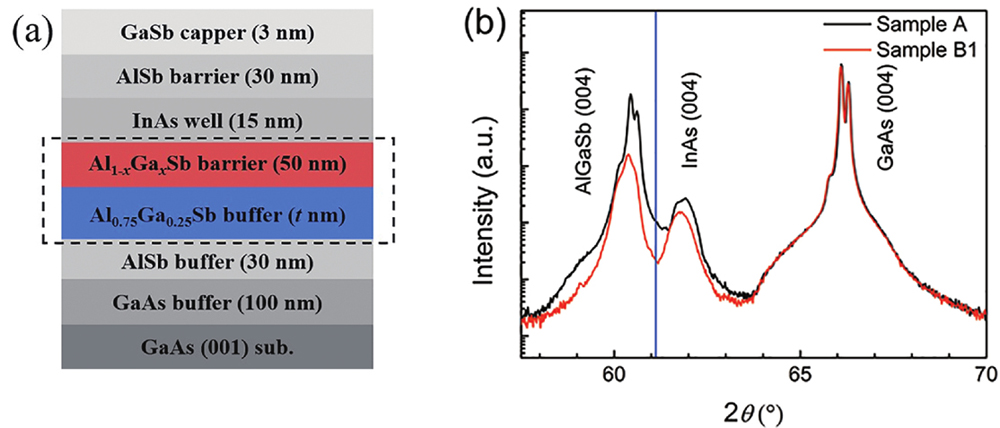
    Fig. 1. (Color online) (a) Layer structure and (b) XRD curves of (Al,Ga)Sb/InAs 2DEGs. The blue line in (b) indicates the calculated diffraction angle of unstrained InAs (004) plane.
    (Color online) AFM images (5 × 5 μm2) of (a) sample A, (b) sample B1, (c) sample B2, (d) sample B3, and (e) sample B4. The left-hand and right-hand images in (a)–(e) correspond to the 2D and 3D surface morphology, respectively.
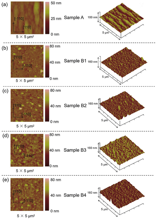
    Fig. 2. (Color online) AFM images (5 × 5 μm2) of (a) sample A, (b) sample B1, (c) sample B2, (d) sample B3, and (e) sample B4. The left-hand and right-hand images in (a)–(e) correspond to the 2D and 3D surface morphology, respectively.
    (Color online) (a) Schematic diagram of Hall bar devices with the current along the [–110] and [110] directions. (b) Sheet resistances as a function of temperature, (c) Hall resistances as a function of magnetic field, and (d) electron sheet concentrations as a function of temperature along the [–110] and [110] directions for sample A.
    Fig. 3. (Color online) (a) Schematic diagram of Hall bar devices with the current along the [–110] and [110] directions. (b) Sheet resistances as a function of temperature, (c) Hall resistances as a function of magnetic field, and (d) electron sheet concentrations as a function of temperature along the [–110] and [110] directions for sample A.
    (Color online) (a) Temperature dependence of electron mobilities along the [–110] and [110] directions for sample A. (b)μ[–110]/μ[110] and NS[–110]/NS[110] as a function of temperature for sample A.
    Fig. 4. (Color online) (a) Temperature dependence of electron mobilities along the [–110] and [110] directions for sample A. (b)μ[–110]/μ[110] and NS[–110]/NS[110] as a function of temperature for sample A.
    (Color online) (a) Temperature dependence of μ[–110]/μ[110] and NS[–110]/NS[110] for sample B1. (b) μ[–110]/μ[110] as a function of temperature for samples B1–B4.
    Fig. 5. (Color online) (a) Temperature dependence of μ[–110]/μ[110] and NS[–110]/NS[110] for sample B1. (b) μ[–110]/μ[110] as a function of temperature for samples B1–B4.
    ParameterASeries-B
    B1B2B3B4
    t (nm) ~ 1000~ 120~ 120~ 120~ 120
    x~ 0~ 0~ 0.2~ 0.4~ 0.6
    Table 1. Detailed information of A and series-B samples.
    Qiqi Wei, Hailong Wang, Xupeng Zhao, Jianhua Zhao. Electron mobility anisotropy in (Al,Ga)Sb/InAs two-dimensional electron gases epitaxied on GaAs (001) substrates[J]. Journal of Semiconductors, 2022, 43(7): 072101
    Download Citation