Abstract
The electron mobility anisotropy in (Al,Ga)Sb/InAs two-dimensional electron gases with different surface morphology has been investigated. Large electron mobility anisotropy is found for the sample with anisotropic morphology, which is mainly induced by the threading dislocations in the InAs layer. For the samples with isotropic morphology, the electron mobility is also anisotropic and could be attributed to the piezoelectric scattering. At low temperature (below transition temperature), the piezoelectric scattering is enhanced with the increase of temperature, leading to the increase of electron mobility anisotropy. At high temperature (above transition temperature), the phonon scattering becomes dominant. Because the phonon scattering is isotropic, the electron mobility anisotropy in all the samples would be reduced. Our results provide useful information for the comprehensive understanding of electron mobility anisotropy in the (Al,Ga)Sb/InAs system.The electron mobility anisotropy in (Al,Ga)Sb/InAs two-dimensional electron gases with different surface morphology has been investigated. Large electron mobility anisotropy is found for the sample with anisotropic morphology, which is mainly induced by the threading dislocations in the InAs layer. For the samples with isotropic morphology, the electron mobility is also anisotropic and could be attributed to the piezoelectric scattering. At low temperature (below transition temperature), the piezoelectric scattering is enhanced with the increase of temperature, leading to the increase of electron mobility anisotropy. At high temperature (above transition temperature), the phonon scattering becomes dominant. Because the phonon scattering is isotropic, the electron mobility anisotropy in all the samples would be reduced. Our results provide useful information for the comprehensive understanding of electron mobility anisotropy in the (Al,Ga)Sb/InAs system.Introduction
Two-dimensional electron gases (2DEGs) are attractive systems for the study of novel physical phenomena, such as quantum Hall effect[1, 2] and topological superconductivity[3, 4]. Additionally, 2DEGs show a huge potential for fabricating devices with diverse functionalities, including light-emitting diodes[5, 6] and magnetic sensors[7, 8]. Among these 2DEGs, the (Al,Ga)Sb/InAs system has attracted much attention due to its unique physical properties[9]. Specifically, the large conduction-band offset (~ 1.35 eV) between AlSb and InAs prevents the electron tunneling from the InAs well into other layers, which reduces the leakage current in AlSb/InAs-based devices[10]. In addition, the band configuration of (Al,Ga)Sb/InAs heterostructures can be tuned by varying the chemical composition of (Al,Ga)Sb barrier, giving flexibility for the design of various photodetectors and diode lasers[11, 12]. Moreover, InAs quantum well is a promising platform for the development of magnetic semiconductors with high Curie temperature and also as an ideal channel material for spin field-effect transistors, which are useful in spintronics[13-15]. Electron mobility is one of the most important physical parameters for the 2DEG systems. In (Al,Ga)Sb/InAs 2DEGs, the electron mobility could reach as high as 30000 cm2/(V·s) at 300 K, which makes this system suitable for the high electron mobility transistors (HEMTs)[16, 17].
When AlSb/InAs 2DEGs are grown on (001)-oriented substrates, the electron mobility is found to be dependent on the crystal direction, showing an anisotropic behavior[18, 19]. In detail, the electron mobility is the highest along the [–110] direction, and the lowest along the [110] direction[18, 19]. As revealed by many works, the anisotropic electron mobility in 2DEGs based on III–V semiconductors could be induced by the anisotropic morphology, which is further related to the anisotropy of lattice relaxation[20] or interface roughness[21]. However, in some cases, the electron mobility of 2DEGs with isotropic morphology is also anisotropic[22]. This suggests that there are other physical origins of the anisotropic electron mobility. In previous works, the electron mobility anisotropy of AlSb/InAs 2DEGs is simply attributed to the anisotropic morphology[18]. However, other possible origins of electron mobility anisotropy in this system have not yet been explored and a more comprehensive study is still lacking.
In this study, we investigate the electron mobility anisotropy of AlSb/InAs/(Al,Ga)Sb 2DEGs by changing the thickness of Al0.75Ga0.25Sb buffer layer and chemical composition of Al1–xGaxSb bottom barrier. Large electron mobility anisotropy is found in the sample with anisotropic morphology (thicker Al0.75Ga0.25Sb buffer layer), which is consistent with previous reports[18, 19]. A relatively small electron mobility anisotropy is also observed in the samples with isotropic morphology (thinner Al0.75Ga0.25Sb buffer layer) and is inferred to originate from the piezoelectric (PE) scattering. Our results address the important influence of PE scattering on the electron mobility anisotropy in the (Al,Ga)Sb/InAs system, and are valuable for a deeper understanding of this issue.
Sample growth
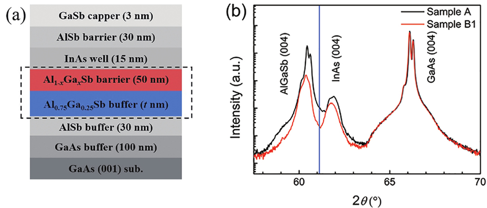
The AlSb/InAs/Al1–xGaxSb 2DEG samples (named as samples A and B1–B4) were grown on GaAs (001) substrates by molecular-beam epitaxy. The layer structure is shown in Fig. 1(a), and the sample information is listed in Table 1. During the growth of the AlSb/InAs/Al1–xGaxSb heterostructures, an appropriate shutter sequence was used to form InSb-like interfaces[23]. For all the samples, the growth conditions are nominally identical except for the thickness of Al0.75Ga0.25Sb buffer layer and the chemical composition of Al1–xGaxSb bottom barrier. In sample A, the thickness of Al0.75Ga0.25Sb buffer layer is ~ 1000 nm and the bottom barrier is AlSb layer. In samples B1–B4, the thickness of Al0.75Ga0.25Sb buffer layer is ~ 120 nm and the chemical composition of the Al1–xGaxSb bottom barrier is x ~ 0 (sample B1), x ~ 0.2 (sample B2), x ~ 0.4 (sample B3), and x ~ 0.6 (sample B4), respectively. Fig. 1(b) presents the X-ray diffraction (XRD) θ–2θ results of samples A and B1, and the wavelength of X-ray is ~ 1.5406 Å. The blue line in Fig. 1(b) shows the calculated diffraction angle of the InAs (004) plane, which suggests that the InAs layers in the two samples are both in-plane tensile-strained. For sample A, the InAs (004) diffraction angle is larger, indicating the larger in-plane tensile strain in the InAs layer and the larger in-plane lattice constant of the Al0.75Ga0.25Sb buffer layer. This result is related to the strain relaxation in the Al0.75Ga0.25Sb buffer layer. Due to the large lattice mismatch between GaAs (~ 5.65 Å) and Al0.75Ga0.25Sb (~ 6.1 Å), the initial Al0.75Ga0.25Sb layer is highly strained during the growth. When the thickness of Al0.75Ga0.25Sb layer is increased, the compressive strain could be gradually released by the formation of dislocations. Thus, more strain in the Al0.75Ga0.25Sb layer of sample A is relaxed, resulting in the larger in-plane lattice constant of the Al0.75Ga0.25Sb layer. Furthermore, the less compressive strain in the Al0.75Ga0.25Sb layer leads to the smaller out-of-plane lattice constant of Al0.75Ga0.25Sb and larger diffraction angle of the Al0.75Ga0.25Sb (004) plane, which is consistent with the results of Fig. 1(b).
Table Infomation Is Not Enable

Figure 1.(Color online) (a) Layer structure and (b) XRD curves of (Al,Ga)Sb/InAs 2DEGs. The blue line in (b) indicates the calculated diffraction angle of unstrained InAs (004) plane.
As shown in Figs. 2(a)–2(e), the surface morphology of these samples is characterized by atomic force microscope (AFM). The root mean square (RMS) values of all the samples are 1.97 nm (sample A), 3.65 nm (sample B1), 4.35 nm (sample B2), 4.55 nm (sample B3), and 3.55 nm (sample B4), respectively. These values indicate that the sample with a relatively thicker Al0.75Ga0.25Sb buffer layer has a smoother surface. However, as shown by the AFM images, the morphology of the sample with thick buffer layer is anisotropic (see Fig. 2(a)), while the samples with thinner buffer layer show isotropic surface (see Figs. 2(b)–2(e)). For sample A, there are some trenches along the [–110] direction on the surface of GaSb capping layer. It is reported that the trenches are induced by the threading dislocations originating from the AlSb/GaAs interface[18, 19]. These dislocations could propagate throughout the whole structure, which induces the [–110]-oriented trenches in the InAs channel, and the trenches then extend to the sample surface[18, 19]. The surface morphology of samples B1–B4 is very similar: the trenches are unclear but a high density of mounds are randomly distributed on the surface. The AFM images indicate that, compared with the chemical composition of Al1–xGaxSb barrier, the thickness of Al0.75Ga0.25Sb buffer layer has a more significant impact on the surface morphology anisotropy.
Figure 2.(Color online) AFM images (5 × 5 μm2) of (a) sample A, (b) sample B1, (c) sample B2, (d) sample B3, and (e) sample B4. The left-hand and right-hand images in (a)–(e) correspond to the 2D and 3D surface morphology, respectively.
Magneto-transport measurements
The samples are patterned into Hall-bar devices with the current flowing in the [–110] and [110] directions, as schematically shown inFig. 3(a). The channel width is 50 μm and the distance between two adjacent electrodes along the channel direction (like electrodes 1 and 2) is 500 μm. During the magneto-transport measurement, the resistances along these two directions are measured simultaneously to reduce the experimental error. Fig. 3(b) presents the temperature dependence of sheet resistance (RS) with the current applied along the [–110] and [110] directions for sample A. The sheet resistance shows a strong dependence on the crystal direction, and the values of sheet resistance are found to be larger when the current is along the [110] direction, which suggests the anisotropy of the electrical properties in (Al,Ga)Sb/InAs system.Fig. 3(c) shows the Hall resistance (Ryx) as a function of the magnetic field at selective temperatures. Through fitting the Hall data using a linear function, the electron sheet concentration (NS) can be obtained from the slope of the Ryx–H curve. The fitting results for the current applied along the [–110] and [110] directions are shown inFig. 3(d), and the electron sheet concentrations are almost the same. Fig. 4(a) presents the temperature dependence of the electron mobility along the [–110] and [110] directions. Compared with the [110] direction, the electron mobility is higher when the current is along the [–110] direction in the temperature range of 10–300 K, showing that the electron mobility is anisotropic. To quantitatively describe the anisotropy in the electrical properties, we introduce two parameters:α = μ[–110]/μ[110] and β = NS[–110]/NS[110], whose temperature dependence are shown in Fig. 4(b). The values of α decrease with the increase of temperature, while the values of β are about 1 in the whole temperature range. The electron mobility anisotropy in this sample could be directly attributed to the trenches in the InAs layer. As discussed earlier, the trenches observed on the surface suggest the presence of trenches in the InAs layer[19]. It is reported that the scattering from the trenches has a more significant impact on the electrons moving in the direction perpendicular to the trenches, leading to an anisotropic scattering of electrons[19]. Since the trenches are nearly parallel with the [–110] direction, the electron scattering from these trenches in the InAs layer is stronger than that along the [110] direction (that isμ[–110] > μ[110]).
Figure 3.(Color online) (a) Schematic diagram of Hall bar devices with the current along the [–110] and [110] directions. (b) Sheet resistances as a function of temperature, (c) Hall resistances as a function of magnetic field, and (d) electron sheet concentrations as a function of temperature along the [–110] and [110] directions for sample A.
Figure 4.(Color online) (a) Temperature dependence of electron mobilities along the [–110] and [110] directions for sample A. (b)μ[–110]/μ[110] and NS[–110]/NS[110] as a function of temperature for sample A.
The transport properties of sample B1 with thinner Al0.75Ga0.25Sb buffer layer are presented in Fig. 5(a). At all the temperatures, the electron sheet concentrations along the two directions are slightly different, which may be attributed to the existence of different scattering sources in these two orthogonal directions or the inhomogeneous distribution of traps in the sample[24]. Further studies are still required to clarify the observed electron density anisotropy. The values of β have a negligible temperature dependence, which is similar to that of sample A. However, the temperature dependence of α for samples A and B1 is obviously different. Compared with sample A, α in sample B1 is smaller in the whole temperature range and shows a non-monotonic variation with the temperature. At low temperature (T < 50 K), α increases with the increase of temperature. When the temperature is further increased, α begins to decrease, showing a maximum around 50 K. These results indicate that the magnitude and temperature dependence of the electron mobility anisotropy in (Al,Ga)Sb/InAs 2DEGs could be significantly influenced by the thickness of buffer layer, the reasons for which are analyzed as follows.
Figure 5.(Color online) (a) Temperature dependence of μ[–110]/μ[110] and NS[–110]/NS[110] for sample B1. (b) μ[–110]/μ[110] as a function of temperature for samples B1–B4.
First, we concentrate on the magnitude of electron mobility anisotropy. As mentioned above, the [–110]-oriented trenches in InAs layer could cause the electron mobility anisotropy. For sample A, there are very clear trenches on the surface (seeFig. 2(a)), implying a higher density of threading dislocations in the InAs layer. This inference should be reasonable because thicker Al0.75Ga0.25Sb layer is more likely to release the mismatch strain by the formation of dislocations. Consequently, the much higher density of threading dislocations forms more trenches in the InAs layer, leading to the larger electron mobility anisotropy in sample A. For samples A and B1, the electron mobility anisotropy could also originate from the PE scattering[25, 26]. As studied by many theoretical works, the PE scattering mechanism resulting from the shear strain limits the electron mobility at low temperature in the strained quantum wells[25, 26]. For an ideal (001)-oriented strained quantum well with the zinc-blende structure, in which the barrier/well interface is absolutely flat, the strain field in the electron well has no shear components[27]. Because the interface roughness could modify the strain field, the shear strain is actually present in the electron well layer with a rough barrier/well interface[25, 26]. Moreover, this non-zero shear strain can give rise to a piezoelectric field, leading to the piezoelectric scattering[25, 26]. The mobility limited by the piezoelectric scattering can be expressed as:
, in which e14, ε, Δ and Λ are the piezoelectric coefficient, the average normal strain, the interface randomness amplitude and the correlation length, respectively[28]. Based on this model, the PE scattering can be anisotropic owing to the different correlation lengths in the [−110] and [110] directions[22, 29]. By comparing the magnitude of anisotropic electron mobility in samples A and B1, it can be inferred that the scattering from trenches has a greater impact on the electron mobility anisotropy than the PE scattering.
Second, we focus on the temperature dependence of electron mobility anisotropy. With the increase of temperature, the phonon scattering is enhanced and becomes dominant. Because the phonon scattering is isotropic, α would decrease when the temperature is increased[28]. In addition, the scattering from the trenches in InAs layer should also influence the temperature dependence of α[19]. The increase of temperature reduces the electron mean free path for both two directions, which would make the effect of trenches on the electron mobility weaker and reduce the electron mobility anisotropy[19]. In sample A, the phonon scattering and the scattering from the trenches in InAs layer should be the dominant scattering mechanisms that influence the temperature dependence of electron mobility anisotropy, thus α decreases monotonically when the temperature is increased. In sample B1 with isotropic morphology, the temperature dependence of electron mobility anisotropy is mainly affected by the PE scattering and the phonon scattering. For the PE scattering, the piezoelectric coefficient e14 usually varies with the temperature[30, 31], so the PE scattering is temperature dependent. For example, the piezoelectric coefficient e14 is found to be proportional to the temperature in the InxGa1–xAs well[30, 31]. With increasing In composition from 0.12 to 0.21, the temperature dependence of piezoelectric coefficient becomes stronger[32]. In consideration of the similarity between InxGa1–xAs and InAs, it is natural to infer that the piezoelectric coefficient of InAs layer might also have a similar temperature dependence. Therefore, when the temperature is increased at low temperature range (T < 50 K), the PE scattering becomes more significant and leads to an enhanced electron mobility anisotropy [28].
As presented in Fig. 5(b), the electron mobility anisotropy of samples B2–B4 also shows a non-monotonic temperature dependence, which is similar with that of sample B1. As the surface morphology of samples B1-B4 is quite similar, the observed non-monotonic temperature dependence of electron mobility anisotropy in samples B2–B4 should also originate from the competition of isotropic phonon scattering and anisotropic PE scattering. Interestingly, the transition temperatures corresponding to the maximums in the α–T curves are obviously different in these samples. With increasing Ga composition, the transition temperature increases, suggesting that the strength of PE scattering could be affected by the chemical composition of the Al1–xGaxSb bottom barrier. The variation of chemical composition in Al1–xGaxSb layer changes the lattice constant of Al1–xGaxSb, which would have an impact on the average normal strain ε in the InAs layer. Furthermore, the strain in Al1–xGaxSb is also influenced by the lattice constant of Al1–xGaxSb, leading to different surface morphology of Al1–xGaxSb layers[33], which might modify the randomness amplitude Δ and the correlation length Λ at the Al1–xGaxSb/InAs interface. For quantitative analysis of the PE scattering mechanism in the Al1–xGaxSb/InAs 2DEGs, the Al1–xGaxSb/InAs interface parameters and the residual strain in the InAs layer need to be further studied.
Conclusion
In conclusion, we have investigated the electron mobility anisotropy in (Al,Ga)Sb/InAs 2DEGs with different surface morphology. The anisotropic morphology is only observed for the sample with thicker Al0.75Ga0.25Sb buffer layer. The surface morphology is highly related to the strain relaxation in the Al0.75Ga0.25Sb layer, as revealed by the XRD results. The sample with the anisotropic morphology shows larger electron mobility anisotropy, which mainly results from the anisotropic electron scattering by the trenches in the InAs layer. The electron mobility anisotropy observed in the samples with the isotropic morphology could be attributed to the PE scattering, which is found to be obviously affected by the composition of Al1-xGaxSb bottom barrier. With the variation of temperature, the competition of isotropic phonon scattering and anisotropic PE scattering leads to the non-monotonic temperature dependence of electron mobility anisotropy. Our results provide useful information on the physical origins of the electron mobility anisotropy, which are helpful for the design of relevant devices based on the (Al,Ga)Sb/InAs 2DEG system.
Acknowledgements
This work is supported by NSFC (Grants No. 11834013 and 12174383). H. L. Wang also acknowledges the support from the Youth Innovation Promotion Association, Chinese Academy of Sciences (No. 2021110).
References
[1] D C Tsui, H L Stormer, A C Gossard. Two-dimensional magnetotransport in the extreme quantum limit. Phys Rev Lett, 48, 1559(1982).
[2] R Willett, J P Eisenstein, H L Störmer et al. Observation of an even-denominator quantum number in the fractional quantum Hall effect. Phys Rev Lett, 59, 1776(1987).
[3] M Kjaergaard, F Nichele, H J Suominen et al. Quantized conductance doubling and hard gap in a two-dimensional semiconductor-superconductor heterostructure. Nat Commun, 7, 1(2016).
[4] J Shabani, M Kjærgaard, H J Suominen et al. Two-dimensional epitaxial superconductor-semiconductor heterostructures: A platform for topological superconducting networks. Phys Rev B, 93, 155402(2016).
[5] J H Lee, J H Lee. Enhanced output power of InGaN-based light-emitting diodes with AlGaN/GaN two-dimensional electron gas structure. IEEE Electron Device Lett, 31, 455(2010).
[6] J H Lee, J H Lee. High-power InGaN-based LED with tunneling-junction-induced two-dimensional electron gas at AlGaN/GaN heterostructure. IEEE Trans Electron Devices, 58, 3058(2011).
[7] A Sandhu, A Okamoto, I Shibasaki et al. Nano and micro Hall-effect sensors for room-temperature scanning hall probe microscopy. Microelectron Eng, 73, 524(2004).
[8] A Sandhu, H Masuda, A Oral et al. Room temperature scanning Hall probe microscopy using GaAs/AlGaAs and Bi micro-hall probes. Ultramicroscopy, 91, 97(2002).
[9] H Kroemer. The 6.1 Å family (InAs, GaSb, AlSb) and its heterostructures: a selective review. Physica E, 20, 196(2004).
[10] A Nakagawa, H Kroemer, J H English. Electrical properties and band offsets of InAs/AlSb n-N isotype heterojunctions grown on GaAs. Appl Phys Lett, 54, 1893(1989).
[11] A Rogalski, P Martyniuk, M Kopytko. InAs/GaSb type-II superlattice infrared detectors: Future prospect. Appl Phys Rev, 4, 031304(2017).
[12] T Hosoda, T Feng, L Shterengas et al. High power cascade diode lasers emitting near 2 μm. Appl Phys Lett, 108, 131109(2016).
[13] P Nam Hai, L Duc Anh, S Mohan et al. Growth and characterization of n-type electron-induced ferromagnetic semiconductor (In, Fe) As. Appl Phys Lett, 101, 182403(2012).
[14] T Dietl, A Bonanni, H Ohno. Families of magnetic semiconductors-an overview. J Semicond, 40, 080301(2019).
[15] B Gu. High temperature magnetic semiconductors: narrow band gaps and two-dimensional systems. J Semicond, 40, 081504(2019).
[16] J B Boos, W Kruppa, B R Bennett et al. AlSb/InAs HEMT's for low-voltage, high-speed applications. IEEE Trans Electron Devices, 45, 1869(1998).
[17] B Y Ma, J Bergman, P Chen et al. InAs/AlSb HEMT and its application to ultra-low-power wideband high-gain low-noise amplifiers. IEEE Trans Microwave Theory Tech, 54, 4448(2006).
[18] G Moschetti, H Zhao, P Å Nilsson et al. Anisotropic transport properties in InAs/AlSb heterostructures. Appl Phys Lett, 97, 243510(2010).
[19] L Desplanque, S El Kazzi, J L Codron et al. AlSb nucleation induced anisotropic electron mobility in AlSb/InAs heterostructures on GaAs. Appl Phys Lett, 100, 262103(2012).
[20] S Löhr, S Mendach, T Vonau et al. Highly anisotropic electron transport in shallow InGaAs heterostructures. Phys Rev B, 67, 045309(2003).
[21] Y Tokura, T Saku, S Tarucha et al. Anisotropic roughness scattering at a heterostructure interface. Phys Rev B, 46, 15558(1992).
[22] M Akabori, T Q Trinh, M Kudo et al. Strain-enhanced electron mobility anisotropy in InxGa1 – xAs/InP two-dimensional electron gases. Physica E, 42, 1130(2010).
[23] Q Q Wei, H L Wang, S C Tong et al. Ga composition effects on the electrical parameters of (Al, Ga) Sb/InAs two-dimensional electron gas. Semicond Sci Technol, 36, 025002(2020).
[24] R S Goldman, H H Wieder, K L Kavanagh et al. Anisotropic structural, electronic, and optical properties of InGaAs grown by molecular beam epitaxy on misoriented substrates. Appl Phys Lett, 65, 1424(1994).
[25] D N Quang, V N Tuoc, N H Tung et al. Random piezoelectric field in real [001]-oriented strain-relaxed semiconductor heterostructures. Phys Rev Lett, 89, 077601(2002).
[26] D N Quang, V N Tuoc, T D Huan. Roughness-induced piezoelectric scattering in lattice-mismatched semiconductor quantum wells. Phys Rev. B, 68, 195316(2003).
[27] E Anastassakis. Strained superlattices and heterostructures: Elastic considerations. J Appl Phys, 68, 4561(1990).
[28] S P Le, T Suzuki. Electron mobility anisotropy in InAs/GaAs (001) heterostructures. Appl Phys Lett, 118, 182101(2021).
[29] T Saku, Y Horikoshi, Y Tokura. Limit of electron mobility in AlGaAs/GaAs modulation-doped heterostructures. Jpn J Appl Phys, 35, 34(1996).
[30] S Cho, A Majerfeld, A Sanz-Hervás et al. Determination of the pyroelectric coefficient in strained InGaAs/GaAs quantum wells grown on (111)B GaAs substrates. J Appl Phys, 90, 915(2001).
[31] J J Sanchez, J I Izpura, J M G Tijero et al. Confirmation of the pyroelectric coefficient of strained InxGa1–xAs/GaAs quantum well structures grown on (111)B GaAs by differential photocurrent spectroscopy. J Appl Phys, 91, 3002(2002).
[32] S Cho, A Majerfeld, J J Sánchez et al. Observation of the pyroelectric effect in strained piezoelectric InGaAs/GaAs quantum-wells grown on (111) GaAs substrates. Microelectron J, 33, 531(2002).
[33] Z H Li, W X Wang, L S Liu et al. Buffer influence on AlSb/InAs/AlSb quantum wells. J Cryst Growth, 301, 181(2007).