
Xin-Xing Fei, Ying Wang, Xin Luo, Cheng-Hao Yu. Simulation study of high voltage GaN MISFETs with embedded PN junction[J]. Chinese Physics B, 2020, 29(8):
- Chinese Physics B
- Vol. 29, Issue 8, (2020)
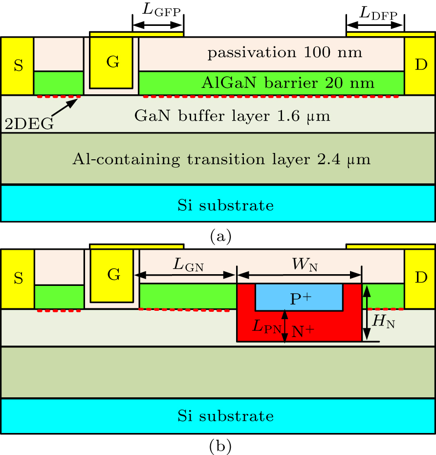
Fig. 1. Schematic diagram of (a) FPC-MISFET and (b) EJ-MISFET.
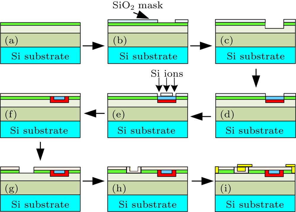
Fig. 2. Schematic diagram of fabrication steps for proposed structure.
Fig. 3. (a) The I D–V DS characteristic curves and (b) blocking characteristic cuves from simulation and experiment to validate effectiveness of models used in simulation.
Fig. 4. Channel electric field distribution of C-MISFET (without field plates), FPC-MISFET, and EJ-MISFET.
Fig. 5. Off-state breakdown voltage from simulation of C-MISFET (without field plate), FPC-MISFET, and EJ-MISFET.
Fig. 6. Lateral electron density distribution in 2DEG for FPC-MISFET and EJ-MISHFET.
Fig. 7. Output characteristics of FPC-MISFET and EJ-MISFET.
Fig. 8. Transfer characteristics of FPC-MISFET and EJ-MISFET.
Fig. 9. Plot of optimized V BK and R ONversus N N+ with N N+ ranging from 6× 1018 cm−3 to 2.4× 1019 cm−3 and L GN taking optimized value.
Fig. 10. Plot of optimized V BK and R ONversus L GN with L GN ranging from 3 μm to 14 μm and N N+ bing 1× 1019 cm−3.
Fig. 11. Plot of V BK and R ONversus W N with W N ranging from 1 μm to 1.8 μm.
Fig. 12. Plot of V BK and R ONversus H N with H N ranging from 36 nm to 71 nm and H P being 31 nm.
Fig. 13. Plot of V BK and R ONversus H P with H P ranging from 23 nm to 37 nm and H N being 41 nm.
Fig. 14. Plot of V BK and R ONversus N P, N P ranging from 1 × 1017 cm−3 to 1 × 1018 cm−3.
|
Table 1. Key structural parameters.
|
Table 2. Comparison of device characteristic between device in this paper and other reported GaN devices.

Set citation alerts for the article
Please enter your email address
© Copyright 2018-2021 | Chinese Laser Press. All Rights Reserved 沪ICP备15018463号-20