• Chinese Physics B
  • Vol. 29, Issue 8, (2020)
Xin-Xing Fei1, Ying Wang2、†, Xin Luo1, and Cheng-Hao Yu2
Author Affiliations
  • 1College of Information and Communication Engineering, Harbin Engineering University, Harbin 5000, China
  • 2Key Laboratory of RF Circuits and Systems, Ministry of Education, Hangzhou Dianzi University, Hangzhou 310018, China
  • show less
    DOI: 10.1088/1674-1056/ab90f7 Cite this Article
    Xin-Xing Fei, Ying Wang, Xin Luo, Cheng-Hao Yu. Simulation study of high voltage GaN MISFETs with embedded PN junction[J]. Chinese Physics B, 2020, 29(8): Copy Citation Text show less

    Abstract

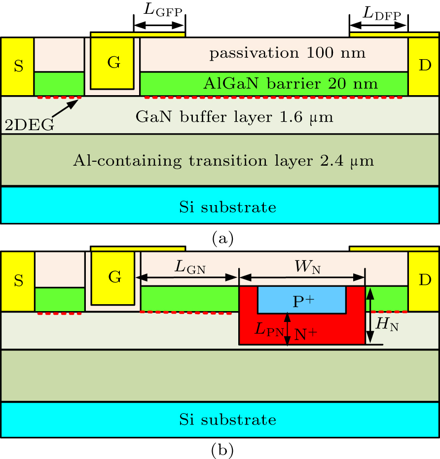
    In this paper, we propose a new enhanced GaN MISFET with embedded pn junction, i.e., EJ-MISFET, to enhance the breakdown voltage. The embedded pn junction is used to improve the simulated device electric field distribution between gate and drain, thus achieving an enhanced breakdown voltage (BV). The proposed simulated device with LGD = 15μm presents an excellent breakdown voltage of 2050 V, which is attributed to the improvement of the device electric field distribution between gate and drain. In addition, the ON-resistance (RON) of 15.37 Ω ?mm and Baliga’s figure of merit of 2.734 GW?cm-2 are achieved in the optimized EJ-MISFET. Compared with the field plate conventional GaN MISFET (FPC-MISFET) without embedded pn junction structure, the proposed simulated device increases the BV by 32.54% and the Baliga’s figure of merit is enhanced by 71.3%.
    Xin-Xing Fei, Ying Wang, Xin Luo, Cheng-Hao Yu. Simulation study of high voltage GaN MISFETs with embedded PN junction[J]. Chinese Physics B, 2020, 29(8):
    Download Citation