• Journal of Semiconductors
  • Vol. 40, Issue 6, 062001 (2019)
Naili Yue1, Joshua Myers2, Liqin Su1, Wentao Wang3, Fude Liu3, Raphael Tsu1, Yan Zhuang2, and Yong Zhang1
Author Affiliations
  • 1Department of Electrical and Computer Engineering, The University of North Carolina at Charlotte, Charlotte, North Carolina 28223, USA
  • 2Department of Electrical Engineering, Wright State University, Dayton, OH 45435, USA
  • 3Department of Mechanical Engineering, The University of Hong Kong, Hong Kong, China
  • show less
    DOI: 10.1088/1674-4926/40/6/062001 Cite this Article
    Naili Yue, Joshua Myers, Liqin Su, Wentao Wang, Fude Liu, Raphael Tsu, Yan Zhuang, Yong Zhang. Growth of oxidation-resistive silicene-like thin flakes and Si nanostructures on graphene[J]. Journal of Semiconductors, 2019, 40(6): 062001 Copy Citation Text show less
    SEM images of epitaxial silicon grown on graphite substrates. (a) and (b) from two areas on S1; (c) and (d) from two areas on S2.
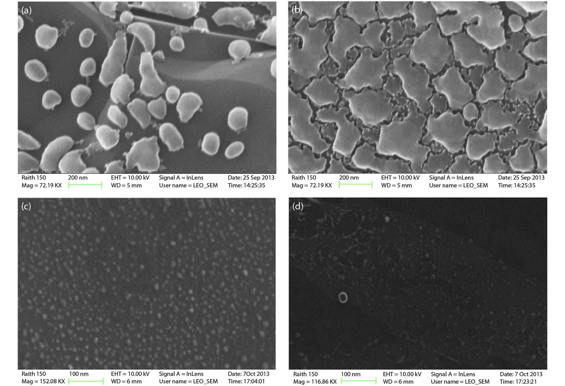
    Fig. 1. SEM images of epitaxial silicon grown on graphite substrates. (a) and (b) from two areas on S1; (c) and (d) from two areas on S2.
    (Color online) AFM and TEM images of epitaxial thin Si film grown on graphite and graphene. (a) and (b) AFM images from samples S1 and S2, respectively. (c) and (d) TEM images from sample S3.
    Fig. 2. (Color online) AFM and TEM images of epitaxial thin Si film grown on graphite and graphene. (a) and (b) AFM images from samples S1 and S2, respectively. (c) and (d) TEM images from sample S3.
    (Color online) Raman spectra of epitaxial thin silicon on graphene. (a) Spectra from two sites on S1, compared with that of bulk Si. (b) Spectra from multiple sites of thin Si films, compared to graphite spectra (inset: an optical image of the area).
    Fig. 3. (Color online) Raman spectra of epitaxial thin silicon on graphene. (a) Spectra from two sites on S1, compared with that of bulk Si. (b) Spectra from multiple sites of thin Si films, compared to graphite spectra (inset: an optical image of the area).
    (Color online) STM images and I–V curves of epitaxial thin silicon on graphite. (a) Current map over a large area containing three types of regions. (b) Comparison of I–V curves of the three types of regions under low bias voltages. (c) and (d) I–V curve and STM image of graphite. (e) and (f) I–V Curve and STM image of ultra-thin silicon. (g) and (h) I–V curve and STM image of thick silicon.
    Fig. 4. (Color online) STM images and I–V curves of epitaxial thin silicon on graphite. (a) Current map over a large area containing three types of regions. (b) Comparison of I–V curves of the three types of regions under low bias voltages. (c) and (d) I–V curve and STM image of graphite. (e) and (f) I–V Curve and STM image of ultra-thin silicon. (g) and (h) I–V curve and STM image of thick silicon.
    Naili Yue, Joshua Myers, Liqin Su, Wentao Wang, Fude Liu, Raphael Tsu, Yan Zhuang, Yong Zhang. Growth of oxidation-resistive silicene-like thin flakes and Si nanostructures on graphene[J]. Journal of Semiconductors, 2019, 40(6): 062001
    Download Citation