
Naili Yue, Joshua Myers, Liqin Su, Wentao Wang, Fude Liu, Raphael Tsu, Yan Zhuang, Yong Zhang. Growth of oxidation-resistive silicene-like thin flakes and Si nanostructures on graphene[J]. Journal of Semiconductors, 2019, 40(6): 062001
- Journal of Semiconductors
- Vol. 40, Issue 6, 062001 (2019)
Abstract
1. Introduction
Since it was first pointed out in 2007 that silicene should have key electronic properties similar to those of graphene[
The feasibility of growing silicene on graphene is supported by a few theoretical modeling results: DFT calculations show that the inter-layer binding between silicene and graphene is stronger than the interlayer–layer bonding of graphene layers in graphite[
Before the recent interest in silicene, some efforts had already been made to grow Si on graphite, for instance, fullerene-structured Si nanowires[
2. Experimental methods and results
In this work, thin Si films were grown on graphite and graphene on SiO2/Si substrates in a MBE system (SVT Associates Inc.) by evaporating bulk Si with an e-beam evaporator. Graphite substrates of a few milimeters size were cleaved from a large single crystal of graphite. Si was deposited in the central region of the small graphite substrate. Since there is very little difference between a graphene and graphite when they are used as a substrate, graphite could be viewed as one layer of graphene supported by a large number of stacked graphene layers with weak bonding, similar to graphene on another supporting material, such as SiO2. Therefore, we will refer to both graphite and graphene on SiO2 as graphene substrate. The typical growth conditions are as follows: growth chamber base pressure being 2 × 10⁻⁸ Torr; heating the substrate to the growth temperature Tg = 800 or 850 °C and held for 15 min; e-beam evaporator running with acceleration voltage 6.07 kV, emission current 150 mA, and filament current 31 A; growth time tg = 15 or 10 min; holding at Tg for 5 min; cooling rate 10 °C/min from Tg to 500 °C, then cooled down naturally to room temperature in the growth chamber.
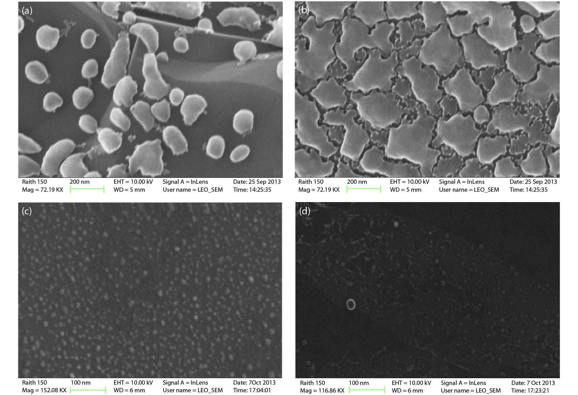
Surface morphology was characterized by SEM and AFM. Si particles and thin-film-like structures were found to form on the cleaved graphite surface that exhibited various clean and flat regions more than 10 μm in size. These regions provide high quality single crystalline graphene to serve as template for epitaxial growth. Transferred graphene on other types of substrates is likely more defective, either due to the presence of polycrystalline domains or chemical residues associated with the transfer. A few typical SEM images are shown in Fig. 1. Figs. 1(a) and 1(b) were taken from sample S1 with Tg/tg = 800 °C/15 min, showing two areas of different densities of Si particles or islands, roughly 100–200 nm in size. Figs. 1(c) and 1(d) from sample S2 with Tg/tg = 850 °C/10 min, showing one area with very small Si particles in the order of 10 nm, and a thin-film like structure of a few μm in size, possibly with embedded small Si particles. The heights of these Si structures were found to be typically in the range of 1 to 15 nm measured by AFM, as shown in the two representative AFM images: Figs. 2(a) and 2(b). Another sample (S3) grown on a graphene/SiO2/Si substrate was examined by TEM, which indicates that Si nanocrystals, typically a few nm in size, were observed on the surface. Fig. 2(c) is a low magnification image, showing Si layer deposited on the graphene/SiO2 substrate. Fig. 2(d) is a high resolution image with visible Si lattice planes of a single Si nanocrystal, but the graphene layer is too thin to see.
![]()
Figure 1.SEM images of epitaxial silicon grown on graphite substrates. (a) and (b) from two areas on S1; (c) and (d) from two areas on S2.
![]()
Figure 2.(Color online) AFM and TEM images of epitaxial thin Si film grown on graphite and graphene. (a) and (b) AFM images from samples S1 and S2, respectively. (c) and (d) TEM images from sample S3.
The epitaxial Si structures were characterized by confocal microRaman using a Horiba LabRam HR800 Raman microscope with a 100× lens (NA = 0.9), excited with a 532 nm laser. A sufficiently low laser power (~ 1 mW) was used to minimize heating induced peak shift. Fig. 3 shows a few representative Raman spectra from the Si on graphite samples. Fig. 3(a) is from S1 measured on two areas: one with a Si particle and the other a uniform area, compared with a bulk Si. In contrast to the severely distorted Raman spectra reported for Si nanoparticles also grown on graphite[
![]()
Figure 3.(Color online) Raman spectra of epitaxial thin silicon on graphene. (a) Spectra from two sites on S1, compared with that of bulk Si. (b) Spectra from multiple sites of thin Si films, compared to graphite spectra (inset: an optical image of the area).
Based on the phonon frequency change between diamond F2g mode (~1300 cm–1) and graphene E2g mode (~1600 cm–1), one would expect that the silicene E2g phonon frequency to be roughly in proportion higher than that of bulk Si at ~520 cm–1. Indeed, the theoretically predicted value for free-standing silicene is 562 cm–1[
It is unusual for the Raman spectra of these very thin Si samples to remain highly stable 2–3 years after the samples were grown. One would expect that such thin Si structures had been mostly oxidized and converted into SiO2, given the oxidation rate of 11–13 Å in one day[
Fig. 4 shows the electrical characterization and STM images for three distinctly different regions on sample S1: of no Si growth (i.e., exposed graphite), of ultra-thin Si (i.e., area with silicene like behavior), and of relatively thick Si. These measurements were acquired using an Agilent AFM 5420 atomic force microscope with a STM nose cone and scanner. The tip was prepared by cutting the wire at a 45° angle prior to lowering into position. The current scans were performed in constant current mode and STM images were obtained in constant height mode. The I–V curves were taken by bringing the tip into contact with the sample at different selected locations of interest, where the tip was held at a constant position and a voltage sweep was performed while measuring the current. The surface of the graphite substrate away from the growth region was used as one contact, and the tip was grounded. Fig. 4(a) is the current map of an area with Si deposition, showing ribbon-like Si structures. The brownish colored area is graphite, the lightest colored area is the thicker Si, whereas the dark area between is the ultra-thin, silicene like Si; as judged by their I–V characteristics and STM images. Note that the strong current contrast revealed in Fig. 4(a) happens because of the very large variations in conductivity between the three regions such that, despite attempting to measure in the constant current mode, the system was unable to maintain a constant current. Fig. 4(b) contrasts the typical I–V characteristics of the three regions under the contact mode. The graphite region is least conductive, then comes the thicker Si region, and finally the silicene-like region is most conductive, with a conductivity of up to 500 times that of the graphite region. For instance, at 3.5 mV the current of the silicene-like region is 370 times that of the graphite region. Also, at ±0.5 V, our conductivity is about a factor of 10 larger than that in the previously reported silicene grown on graphite[
![]()
Figure 4.(Color online) STM images and
3. Discussion
A freshly cleaved Si (111) surface will undergo surface reconstruction if kept in high vacuum, otherwise it will be oxidized into a SiO2 capping layer. In either case, the surface modification is to remove the dangling bonds or minimize the surface energy. Besides SiO2, hydrogen atoms are often used to passivate the dangling bonds in Si. These processes apply to a thick bulk Si. When the layer is sufficiently thin and electronically coupled to a substrate, charge transfer across the heterostructure interface may drastically change the picture. If a very thin Si slab remains in its idealistic sp3 bonding, then it will have one dangling bond on the top layer and one on the bottom layer. There are at least two ways to mitigate the dangling bonds: (1) If the slab is only one monolayer thick, then partially collapsing the buckled (111) monolayer will allow the upper and lower dangling bonds to form a partial π bond, yielding the so-called silicene that is in-principle structurally stable, although it remains chemically unstable (because the weak partial π bond is susceptible to chemical reaction). In contrast, a fully collapsed diamond (111) monolayer forms a much stronger π bond, namely graphene, and thus is chemically much more stable. (2) Accepting charge from the substrate to passivate the dangling bonds, which has been shown to be theoretically possible for a silicene/graphene superlattice[
4. Summary
The ability to grow a single-crystalline thin Si film on graphene substrate opens up new avenues for future generation Si electronic devices. It is highly desirable for fabricating flexible Si based devices being able to perform either pre- or post-growth transfer of graphene or graphene with the grown Si structures to different substrates. Before a large and uniform graphene substrate is available, it might be challenging to grow a large and continuous thin Si film. However, it may not be necessary after all if the goal is to make nanoscale Si devices because a large film is only needed for the traditional top–down approach. This work suggests the possibility to selectively deposit high quality nanoscale Si structures: silicene, a-few-layer silicene, and Si nanocrystals, using a template of nanoscale graphene structures. For instance, one possible way to obtain such a template could be to first grow an array of SiC nanostructures on a large Si wafer and then convert them into graphene nanostructures with a laser beam[
The exact epitaxial relationship between the epitaxial Si structures and the graphene layer is yet to be determined. This is largely true for the epitaxial growth on graphene in general. Si on graphene can provide a simpler model system for understanding the van der Waals epitaxy. We expect that this work will inspire future research and exploration in both applied and fundamental areas, such as semiconductor nanostructures and devices, surface science, and surface passivation.
Acknowledgement
The work at UNCC was supported by ARO/Materials Science (Grant No. W911NF-10-1-0281 and W911NF-18-1-0079, managed by Dr. Chakrapani Varanasi). We thank Dr. Weijie Lu for providing the single crystal graphite, Dr. Chun-Sheng Jiang for helpful discussions on STM, Drs. Kai Wang and Gerd J. Duscher for attempting to identify the epitaxial relationship between the substrate and Si structures. YZ acknowleges the support of Bissell Distinguished Professorship.
References
[1] G G Guzm-Verri, L C Lew Yan Voon. Electronic structure of silicon-based nanostructures. Phys Rev B, 76, 075131(2007).
[2] P Vogt, P De Padova, C Quaresima et al. Silicene: compelling experimental evidence for graphenelike two-dimensional silicon. Phys Rev Lett, 108, 155501(2012).
[3] A Fleurence, R Friedlein, T Ozaki et al. Experimental evidence for epitaxial silicene on diboride thin Films. Phys Rev Lett, 108, 245501(2012).
[4] E Cinquanta, E. Scalise, D Chiappe et al. Getting through the nature of silicene: an sp2-sp3 two-dimensional silicon nanosheet. J Phys Chem C, 117, 16719(20113).
[5] J A Yan, R Stein, D M Schaefer et al. Electron-phonon coupling in two-dimensional silicene and germanene. Phys Rev B, 88, 121403(2013).
[6] E Scalise, M Houssa, G Pourtois et al. Vibrational properties of silicene and germanene. Nano Res, 6, 19(2013).
[7] D Solonenko, O Gordan, G L Lay et al. 2D vibrational properties of epitaxial silicene on Ag(111). 2D Mater, 4, 015008(2017).
[8] J Zhuang, X Xu, Y Du et al. Investigation of electron–phonon coupling in epitaxial silicene by in situ Raman spectroscopy. Phys Rev B, 91, 161409(2015).
[9] S Sheng, J B Wu, X Cong et al. Vibrational properties of a monolayer silicene sheet studied by tip-enhanced Raman spectroscopy. Phys Rev Lett, 119, 196803(2017).
[10] J B Wu, M L Lin, X Cong et al. Raman spectroscopy of graphene-based materials and its applications in related devices. Chem Soc Rev, 47, 1822(2018).
[11] P De Padova, C Ottaviani, C Quaresima et al. 24 h stability of thick multilayer silicene in air. 2D Mater, 1, 021003(2014).
[12] Y Zhang, R Tsu. Binding graphene sheets together using silicon: graphene/silicon superlattice. Nanoscale Res Lett, 5, 805(2010).
[13] R Neuendorf, R E Palmer, R Smith. Low energy deposition of size-selected Si clusters onto graphite. Chem Phys Lett, 333, 304(2001).
[14] Y Cai, C P Chuu, C M Wei et al. Stability and electronic properties of two-dimensional silicene and germanene on graphene. Phys Rev B, 88, 245408(2013).
[15] S Yu, X D Li, S Q Wu et al. Novel electronic structures of superlattice composed of graphene and silicene. Mater Res Bull, 50, 268(2014).
[16] S Fahy, S G Louie, M L Cohen. Pseudopotential total-energy study of the transition from rhombohedral graphite to diamond. Phys Rev B, 34, 1191(1986).
[17] J Wang, Y Zhang. Topologic connection between 2-D layered structures and 3-D diamond structures for conventional semiconductors. Sci Rep, 6, 24660(2016).
[18]
[19] M De Crescenzi, I Berbezier, M Scarselli et al. Formation of silicene nanosheets on graphite. ACS Nano, 10, 11163(2016).
[20] Y Li, H Wang, L Xie et al. MoS2 nanoparticles grown on graphene: an advanced catalyst for the hydrogen evolution reaction. J Am Cheml Soc, 133, 7296(2011).
[21] M M Ugeda, A J Bradley, S F Shi et al. Giant bandgap renormalization and excitonic effects in a monolayer transition metal dichalcogenide semiconductor. Nat Mater, 13, 1091(2014).
[22] C W Teplin, M P Paranthaman, T R Fanning et al. Heteroepitaxial film crystal silicon on Al2O3: new route to inexpensive crystal silicon photovoltaics. Energy Environ Sci, 4, 3346(2011).
[23] K Zhang, J H Seo, W D Zhou et al. Fast flexible electronics using transferrable silicon nanomembranes. J Phys D, 45, 143001(2012).
[24] B Marsen, K Sattler. Fullerene-structured nanowires of silicon. Phys Rev B, 60, 11593(1999).
[25] K G Nath, I Shimoyama, T Sekiguchi et al. Chemical-state analysis for low-dimensional Si and Ge films on graphite. J Appl Phys, 94, 4583(2003).
[26]
[27] G Beaucarne, S Bourdais, A Slaoui et al. Impurity diffusion from uncoated foreign substrates during high temperature CVD for thin-film Si solar cells. Sol Energy Mater Sol Cells, 61, 301(2000).
[28] L Wang, H L Tu, S W Zhu et al. Dispersed Si nanoparticles with narrow photoluminescence peak prepared by laser ablated deposition. Chin J Nonferrous Metals, 20, 724(2010).
[29] Y Baba, I Shimoyama, N Hirao et al. Structure of ultra-thin silicon film on HOPG studied by polarization-dependence of X-ray absorption fine structure. Chem Phys Lett, 594, 64(2014).
[30] K Evanoff, A Magasinski, J Yang et al. Nanosilicon-coated graphene granules as anodes for Li-ion batteries. Adv Energy Mater, 1, 495(2011).
[31] L Su, Y Zhang, Y Yu et al. Dependence of coupling of quasi 2-D MoS2 with substrates on substrate types, probed by temperature dependent Raman scattering. Nanoscale, 6, 4920(2014).
[32] L Su, Y Yu, L Cao et al. Effects of substrate type and material-substrate bonding on high-temperature behavior of monolayer WS2. Nano Res, 8, 2686(2015).
[33] L Su, Y Yu, L Cao et al. In situ in situ monitoring of the thermal-annealing effect in a monolayer of MoS2. Phys Rev Appl, 7, 034009(2017).
[34] L X Li, W P Han, W. J B Wu et al. Layer-number dependent optical properties of 2D materials and their application for thickness determination. Adv Funct Mater, 27, 1604468(2017).
[35] V K Malinovsky, V N Novikov, N V Surovtsev et al. Investigation of amorphous states of SiO2 by Raman scattering spectroscopy. Phys Solid State, 42, 65(2000).
[36] M Ivanda, R Clasen, M Hornfeck et al. Raman spectroscopy on SiO2 glasses sintered from nanosized particles. J Non-Cryst Solids, 322, 46(2003).
[37] S I Raider, R Flitsch, M J Palmer. Oxide growth on etched silicon in air at room temperature. J Electrochem Soc, 122, 413(1975).
[38] J D Ryckman, R A Reed, R A Weller et al. Enhanced room temperature oxidation in silicon and porous silicon under 10 keV X-ray irradiation. J Appl Phys, 108, 113528(2010).
[39] S Tongay, T Schumann, A F Hebard. Graphite based Schottky diodes formed on Si, GaAs, and 4H-SiC substrates. Appl Phys Lett, 95, 222103(2009).
[40] D Sinha, J U Lee. Ideal graphene/silicon schottky junction diodes. Nano Lett, 14, 4660(2014).
[41]
[42] Z X Guo, Y Y Zhang, H Xiang et al. Structural evolution and optoelectronic applications of multilayer silicene. Phys Rev B, 92, 201413(2015).
[43] H A Mizes, S I Park, W A Harrison. Multiple-tip interpretation of anomalous scanning-tunneling-microscopy images of layered materials. Phys Rev B, 36, 4491(1987).
[44] S Hembacher, F J Giessibl, J Mannhart et al. Revealing the hidden atom in graphite by low-temperature atomic force microscopy. Proc Natl Acad Sci, 100, 12539(2003).
[45] H Neddermeyer. Scanning tunnelling microscopy of semiconductor surfaces. Rep Prog Phys, 59, 701(1996).
[46] Y Zhang, G M Dalpian, B Fluegel et al. Novel approach to tuning the physical properties of organic-inorganic hybrid semiconductors. Phys Rev Lett, 96, 026405(2006).
[47] N Yue, Y Zhang, R Tsu. Ambient condition laser writing of graphene structures on polycrystalline SiC thin film deposited on Si wafer. Appl Phys Lett, 102, 071912(2013).

Set citation alerts for the article
Please enter your email address
© Copyright 2018-2021 | Chinese Laser Press. All Rights Reserved 沪ICP备15018463号-20