
Shreeniket Joshi, Amirkianoosh Kiani. Hybrid artificial neural networks and analytical model for prediction of optical constants and bandgap energy of 3D nanonetwork silicon structures[J]. Opto-Electronic Advances, 2021, 4(10): 210039-1
- Opto-Electronic Advances
- Vol. 4, Issue 10, 210039-1 (2021)
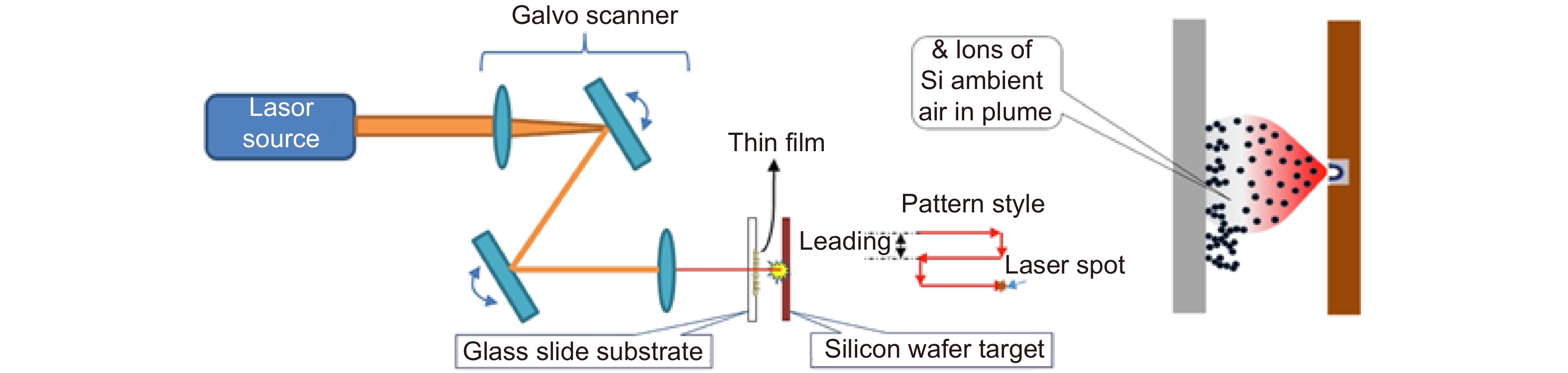
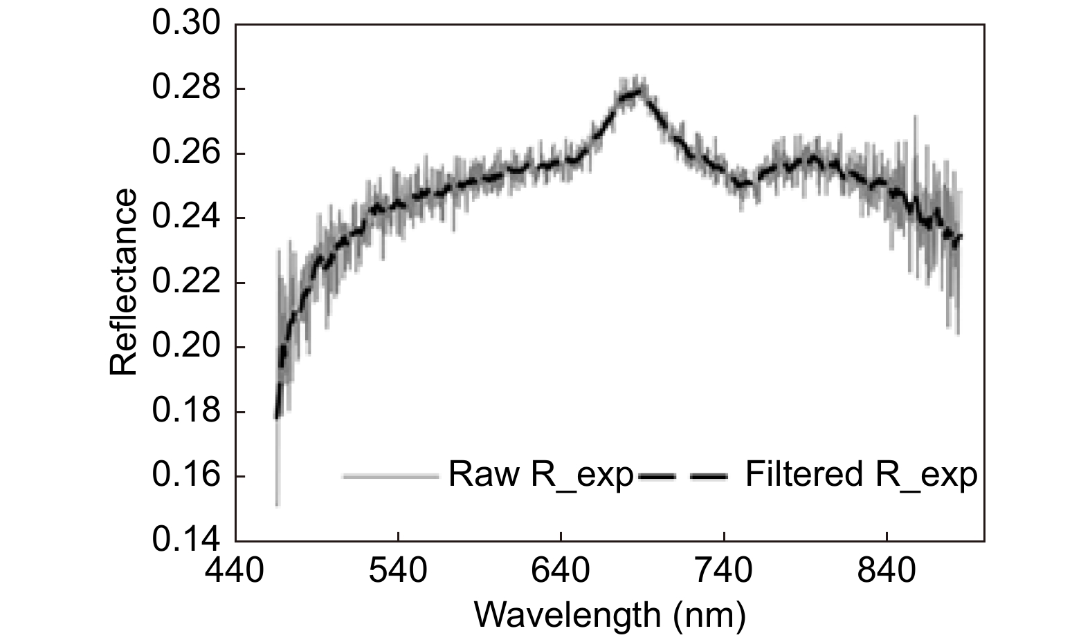
Fig. 2. Filtered reflectance data.
Fig. 3. Filtered transmittance data.
Fig. 4. Model validation with experimental transmittance.
Fig. 5. Refractive index as a function of wavelength.
Fig. 6. Extinction coefficient as a function of wavelength.
Fig. 7. PUMA model validation with analytical refractive index (n ); R_Puma: Simulation results when only reflectance was input; B_Puma: Simulation results when both reflectance and transmittance were inputs.
Fig. 8. PUMA model validation with analytical extinction coefficient (k ).
Fig. 9. PUMA model validation with analytical extinction coefficient (k ).
Fig. 10. PUMA model evaluation with experimental transmittance.
Fig. 11. PUMA model evaluation with experimental reflectance.
Fig. 12. Flowchart for deep learning algorithm.
Fig. 13. Deep Learning Model developed.
Fig. 14. Comparison of model-predicted extinction coefficient with analytical values.
Fig. 15. Comparison of model-predicted refractive index with analytical values.
Fig. 16. Absorption regions for fabricated silicon thin film.
Fig. 17. Tauc’s Plot for determining optical bandgap.
|
Table 1. Prediction of extinction coefficient (k ).
|
Table 2. Prediction of refractive index (n )
|
Table 3. Manufacturing parameters.
|
Table 4. Validation of proposed methodology.
|
Table 5. Band gap information for various silicon structures7


Set citation alerts for the article
Please enter your email address

© Copyright 2018-2021 | Chinese Laser Press. All Rights Reserved 沪ICP备15018463号-20