Journals >Opto-Electronic Advances
Contents


2021
Volume: 4 Issue 10
4 Article(s)
Export citation format
Original Article
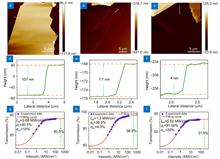
Optical properties and applications of SnS2 SAs with different thickness
Mengli Liu, Hongbo Wu, Ximei Liu, Yaorong Wang, Ming Lei, Wenjun Liu, Wei Guo, and Zhiyi Wei
Q-switched lasers have occupied important roles in industrial applications such as laser marking, engraving, welding, and cutting due to their advantages in high pulse energy. Here, SnS2-based Q-switched lasers are implemented. Considering that SnS2 inherits the thickness sensitive optical characteristics of TMD, threeQ-switched lasers have occupied important roles in industrial applications such as laser marking, engraving, welding, and cutting due to their advantages in high pulse energy. Here, SnS2-based Q-switched lasers are implemented. Considering that SnS2 inherits the thickness sensitive optical characteristics of TMD, three kinds of SnS2 with different thickness are characterized in terms of nonlinearity and used to realize the Q-switched pulses under consistent implementation conditions for comparison tests. According to the results, the influence of thickness variation on the nonlinear performance of saturable absorber, such as modulation depth and absorption intensity, and the influence on the corresponding laser are analyzed. In addition, compared with other traditional saturable absorbers, the advantage of SnS2 in realizing ultrashort pulses is also noticed. Our work explores the thickness-dependent nonlinear optical properties of SnS2, and the rules found is of great reference value for the establishment of target lasers..
Opto-Electronic Advances
- Publication Date: Sep. 25, 2021
- Vol. 4, Issue 10, 200029-1 (2021)


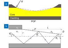
Side-polished SMS based RI sensor employing macro-bending perfluorinated POF
Xuezhi Zhang, Boyue Yang, Junfeng Jiang, Kun Liu, Xiaojun Fan, Zhaozhu Liu, Min Peng, Guanlong Chen, and Tiegen Liu
A refractive index (RI) sensor based on perfluorinated plastic optical fiber (PF-POF) is introduced in this paper. The PF-POF as multi-mode fiber was side-polished (SP) to form a macro-bending single-mode-multimode-single-mode (SMS) structure. Both ends of the sensor were closely connected to single-mode quartz opticalA refractive index (RI) sensor based on perfluorinated plastic optical fiber (PF-POF) is introduced in this paper. The PF-POF as multi-mode fiber was side-polished (SP) to form a macro-bending single-mode-multimode-single-mode (SMS) structure. Both ends of the sensor were closely connected to single-mode quartz optical fiber (SMF). The spectral characteristics of the sensor are measured, analyzed and discussed. The results show that when the length of PF-POF is 8 cm, the macro-bending radius is 3 cm, and the SP-depth is 20 μm. The intensity sensitivity reaches -219.504 dBm/RIU in the range of RI = 1.330 ~ 1.356. A reference is provided for the application of PF-POF in RI sensor in the future. The sensor is featured with low-cost, good flexibility and high efficiency..
Opto-Electronic Advances
- Publication Date: Sep. 25, 2021
- Vol. 4, Issue 10, 200041-1 (2021)
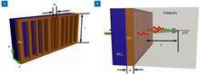
A waveguide metasurface based quasi-far-field transverse-electric superlens
Yechuan Zhu, Xiaolin Chen, Weizheng Yuan, Zhiqin Chu, Kwok-yin Wong, Dangyuan Lei, and Yiting Yu
The imaging capability of conventional lenses is mainly limited by the diffraction of light, and the so-called superlens has been developed allowing the recovery of evanescent waves in the focal plane. However, the remarkable focusing behavior of the superlens is greatly confined in the near-field regime due to the expThe imaging capability of conventional lenses is mainly limited by the diffraction of light, and the so-called superlens has been developed allowing the recovery of evanescent waves in the focal plane. However, the remarkable focusing behavior of the superlens is greatly confined in the near-field regime due to the exponential decay of evanescent waves. To tackle this issue, we design a waveguide metasurface-based superlens with an extraordinary quasi-far-field focusing capability beyond the diffraction limit in the present work. Specifically, we analyze the underlying physical mechanism and provide experimental verification of the proposed superlens. The metasurface superlens is formed by an array of gradient nanoslits perforated in a gold slab, and supports transverse-electric (TE) waveguide modes under linearly polarized illumination along the long axis of the slits. Numerical results illustrate that exciting such TE waveguide modes can modulate not only optical phase but also evanescent waves. Consequently, some high-spatial-frequency waves can contribute to the focusing of the superlens, leading to the quasi-far-field super-resolution focusing of light. Under 405 nm illumination and oil immersion, the fabricated superlens shows a focus spot of 98 nm (i.e. λ/4.13) at a focal distance of 1.49 μm (i.e. 3.68λ) using an oil immersion objective, breaking the diffraction limit of λ/2.38 in the quasi-far field regime. The developed metasurface optical superlens with such extraordinary capabilities promises exciting avenues to nanolithography and ultra-small optoelectronic devices..
Opto-Electronic Advances
- Publication Date: Sep. 25, 2021
- Vol. 4, Issue 10, 210013-1 (2021)

Hybrid artificial neural networks and analytical model for prediction of optical constants and bandgap energy of 3D nanonetwork silicon structures
Shreeniket Joshi, and Amirkianoosh Kiani
The aim of this study is to develop a reliable method to determine optical constants for 3D-nanonetwork Si thin films manufactured using a pulsed-laser ablation technique that can be applied to other materials synthesized by this technique. An analytical method was introduced to calculate optical constants from reflectThe aim of this study is to develop a reliable method to determine optical constants for 3D-nanonetwork Si thin films manufactured using a pulsed-laser ablation technique that can be applied to other materials synthesized by this technique. An analytical method was introduced to calculate optical constants from reflectance and transmittance spectra. Optical band gaps for this novel material and other important insights on the physical properties were derived from the optical constants. The existing optimization methods described in the literature were found to be complex and prone to errors while determining optical constants of opaque materials where only reflectance data is available. A supervised Deep Learning Algorithm was developed to accurately predict optical constants from the reflectance spectrum alone. The hybrid method introduced in this study was proved to be effective with an accuracy of 95%..
Opto-Electronic Advances
- Publication Date: Sep. 25, 2021
- Vol. 4, Issue 10, 210039-1 (2021)

© Copyright 2018-2021 | Chinese Laser Press. All Rights Reserved 沪ICP备15018463号-20