
Shreeniket Joshi, Amirkianoosh Kiani. Hybrid artificial neural networks and analytical model for prediction of optical constants and bandgap energy of 3D nanonetwork silicon structures[J]. Opto-Electronic Advances, 2021, 4(10): 210039-1
- Opto-Electronic Advances
- Vol. 4, Issue 10, 210039-1 (2021)
Abstract
Introduction
Silicon thin films are widely used in semiconductor devices and have numerous applications in opto-electronics, optical devices, bio-medicine and telecommunications
The intensity of light transmitted, absorbed and reflected varies across the electromagnetic spectrum, and changes in response to different incident photon energies. These changes act as important indicators of a material’s properties and can be used to derive insights on intrinsic properties like band gap and dielectric quality. Hence, optical constants are important in benchmarking and finding applications for novel materials
The relation between optical constants is expressed in terms of a Complex Refractive Index (N)
Previous literature studies summarized that optical constants of thin films are widely determined using three methods
1) Ellipsometry data, which is a technique for evaluating the dielectric properties of thin films by measuring the change in polarization after reflection/ transmittance and comparing it to a pre-defined model.
2) Dispersion models.
3) Transmittance and reflectance spectra.
The envelope method was introduced by Manifacier et al
where s is the refractive index of the substrate, d is the thickness of the thin film.
Swanepoel
Swanepoel’s method of analytically determining optical constants from interference fringes is greatly effective in thin films. However, as there no interference fringes in this study, Swanepoel’s method cannot be applied.
Ritter et al
The Cauchy dispersion model
These equations are completely empirical, and as concluded by Poelman et al
The Forouhi-Bloomer (F-B) model as shown in Eqs. (7, 8) is derived from Kramer-Kronig (KK) relations, where Eg represents the optical band gap energy
The F-B method was developed to model the interband region, where photon energies are higher than the bandgap of the material. The values for all the independent variables: Ai, Eg, Bi, Ci, n(∞) in Eqs. (8, 9) should be known
A comprehensive overview of various methods for determination of optical constants has been compiled and compared for accuracy by Poelman et al.
Another method to derive optical constants for thin films involves developing a model for calculating reflectance and transmittance using independent variables, like refractive index of substrate, thickness of film, refractive index of film and extinction coefficient, symbolically represented as s(λ), d, n(λ) and κ(λ) respectively, and equating them to experimentally measured values of transmission and reflectance
If we assume, λ, s(λ) and d to be known, then this problem is reduced to having two unknowns with two equations. However, it is important to emphasize here that n(λ) and κ(λ) are not merely mathematical constants, but have critical physical significance. Hence, there are multiple combinations possible to satisfy the equation which would not be physically acceptable.
Chambouleyron et al
As the thin film discussed in this study is a novel material, it was not possible to obtain information on the nature of its optical properties in terms of optical constants or its response to incident photon energy. Hence, neither PUMA nor any dispersion model could be employed in the preliminary stages of this study. However, once optical constants were determined by the implementation of different analytical models, an attempt to validate this method was made using PUMA, which is described in the Experimental setup and method section.
The current research aims at determining optical constants and using them as indicators to explore material properties of nanofibrous silicon thin films. A novel method involving a combination of three distinct analytical models was introduced; it determines the values of ‘n’ and ‘k’ individually and validates these values by inputting them into an analytical expression for transmittance. Additionally, an Artificial Neural Network (ANN) was built to determine optical constants for opaque materials when only reflectance data is available.
Experimental setup and method
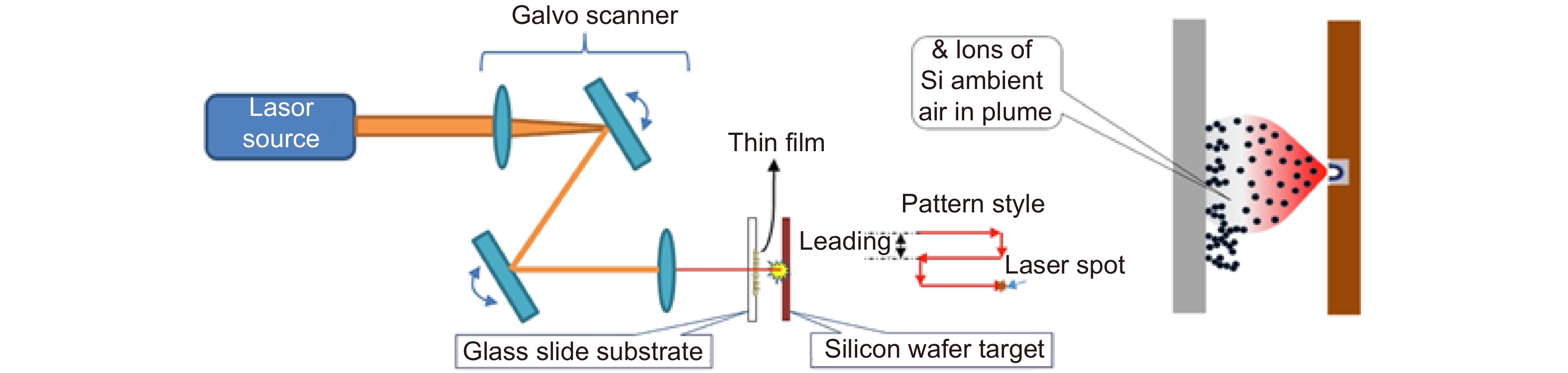
A picosecond Ytterbium pulsed laser (IPG Germany) was used to irradiate a pulsed laser beam onto an n-type silicon wafer, with an orientation of <100> (one side polished-manufactured by Czochralski process). The ablated silicon fibres were deposited on a standard glass slide substrate held in a vertically parallel position. A schematic of the fabrication setup is shown in Fig. 1. A light spectroscopy instrument (Ocean Optics UV-Vis USB 2000+ & STS-NIR) was employed to record reflection and transmission spectra in visible range (400–750 nm) and near-infrared (NIR) range (750–2500 nm), respectively. The details of this fabrication setup, control parameters, mechanism of film ablation and deposition, along with the experimental setup for recording reflection and transmission spectra have been described in a previous study
![]()
Figure 1.
The reflectance and transmittance data included a certain degree of noise. It was important to filter this noise before using the data to determine optical constants and other material properties. Signal smoothing is widely used to improve the signal-to-noise ratio without significantly distorting the signal data. The Savitzky-Golay filter (digital smoothing polynomial/ least square smoothing filter) was employed to track the input data more closely and prevent any transient effects during the smoothing process
In Fig. 2 and Fig. 3, the filtered data is projected onto the experimentally captured data to emphasize the effectiveness of the Savitzky-Golay filter in smoothing the data, at the same time, preserving the essence of the obtained data.
![]()
Figure 2.
![]()
Figure 3.
Results and discussion
Theoretical prediction models
To develop a method to reliably and accurately determine optical constants, different existing analytical methods were tested. A combination of three models was found to provide the most accurate and repeatable results in determining the values of optical constants. This approach is explained below, and comprises Eqs. (11–15).
To make comparisons between different methods, a single sample of silicon nano-fibrous thin films was taken as a standard. The manufacturing parameters for this sample were Power: 10 W, Frequency: 1200 kHz, Pulse duration: 150 ps, and Scanning speed: 100 mm/s. Towards the end of the study, the suggested method was validated against five samples produced with various manufacturing parameters.
An analytical method was adopted which used a combination of different models to determine the values of ‘n’ and ‘k’ individually.
The calculated values of optical constants are then validated by inputting them into an analytical expression for transmittance. In Eqs. (11–15), R: Reflectance, T: Transmittance, d: thickness of thin film, n: refractive index, k: extinction coefficient, α: absorption coefficient.
A relation between absorption coefficient (α) and reflectance and transmittance data, as shown in Eq. (11) was provided by Pankove
This relation was simplified and was successfully applied in the form as shown by Eq. (12) by Vitanov and others
In Eq. (13), experimentally obtained values for R and T are inputted to find absorption coefficient (α). A further extinction coefficient can be found using Eq. (13) as demonstrated in previous publications
Using Eqs. (12) and (13), the values for extinction coefficients (k) were derived for all corresponding wavelengths in the given spectral range. An expression for calculating the refractive index is shown in Eq. (14). This relation employs the previously calculated extinction coefficient, wavelength values and amount of reflectance
It is crucial to validate the accuracy of this analytical approach, and hence an expression for transmittance as shown in Eq. (15) was used. This analytical relation was first provided by Heavens
here subscripts, 0: air, 1: thin film, and 2: substrate. In this case, n0 = 1, n2 = 1.5.
As shown in Fig. 4, the analytically calculated transmittance using the model involving Eqs. (11-15) fits the experimental data perfectly. Experimental transmittance (Trans_exp) and analytically calculated transmittance (Trans_an) were compared and it was found that Sum of Squared Errors (SSE) = 1.4602, Mean Absolute Error (MAE) = 0.020, and Mean Squared Error (MSE) = 0.00114259. As the error is practically zero, it can be inferred that the optical constants determined from the analytical model have been accurately validated with the experimental data.
![]()
Figure 4.
In Figs. 5 and 6, the refractive index and extinction coefficient are plotted as functions of wavelengths. It is important to understand the trend and interdependence between these two properties. For wavelengths between 464 and 514 nm, a decreasing trend in the value for the extinction coefficient can be observed. In this region, the extinction coefficient is at its highest value, and hence the amount of light reflected and transmitted (Figs. 2 and 3) is low, as most of the light is absorbed. It is apparent that a decrease in the value of the extinction coefficient leads to an increase in both reflectance and transmittance values, and hence refractive index is also observed to display an increasing trend. If observed closely, it is evident that the refractive index and the reflectance spectra have a strong interrelation. The trends are exhibited by the refractive index are mimicked by the reflectance spectra. In the region after 750 nm (NIR range), it can be observed that there is a rise in the increasing trend of transmittance. As a result of this, an expected decrease in the refractive index as well as the reflectance spectra is observed. This change in optical properties with wavelength is crucial for developing applications for the novel material discussed in this study. The pulsed-laser fabricated nanofibrous silicon thin film displays strong absorption properties for lower regions of the VIS spectrum and becomes semi-transparent for wavelengths in the NIR range. The nanofibrous silicon thin film developed has strong absorption properties. At 632.8 nm, its extinction coefficient is 0.0044 whereas in a typical sample of Si, it is observed to be 0.01896923 with a refractive index of 3.88. This is substantially higher than the nanofibrous thin film, which has a refractive index of 2.36
![]()
Figure 5.
![]()
Figure 6.
Using the PUMA method
![]()
Figure 7.
![]()
Figure 9.
![]()
Figure 8.
A similar trend was noted when the simulation was implemented for predicting ‘n’ and ‘k’ values from the reflectance spectrum alone. The refractive index was fixed this time after initialization and only the extinction coefficient was varied. Further, the prediction of k values (from reflectance data only) was so erroneous that it could not even be accommodated for comparison in Fig. 8, and a separate Fig. 9 is displayed to show the difference between the actual analytically calculated values and the PUMA prediction for extinction coefficient. The simulation appears to have failed as it is supposed to optimize n and k values for each point.
When the model was analyzed by Mulato et al.
There are two major reasons this method did not work for the above-mentioned nano-fibrous thin films:
1). This method was tested by Mulato et al.
2). As mentioned previously, the numerical approach assumes that n and k are decreasing functions of wavelength, which is not true in this study as it was observed that n(λ) first increases, reaches a peak value and then declines sharply (as shown in Fig. 5).
As discussed earlier, PUMA was implemented to find optical constants from reflectance data only and also to serve as secondary validation for our model.
It can be inferred from Figs. 10 and 11 that when optical constants determined by the PUMA method were inputted into our analytical expressions for reflectance and transmittance, the resulting spectra were for the most part close to the analytical and experimental data. This serves as an important indicator that the analytical expressions for reflectance and transmittance used in our study are very similar to the equations used via unconstrained optimization
![]()
Figure 10.
![]()
Figure 11.
Artificial neural networks
For thin films deposited on opaque substrates, only the reflectance spectrum is available and hence the analytical approach discussed earlier becomes an indeterminant problem. To solve this, it was intended that the thin film would first be deposited on glass substrates and the analytical approach described above would be used to determine the optical constants. This would provide reliable insights about the material’s optical properties. Now the film could be deposited on an opaque substrate, and the reflectance data for this system, consisting of the thin film and the opaque substrates, would be recorded. Thus, the reflectance data combined with knowledge of the optical properties of the nano-fibrous thin film could be used in an optimization algorithm with precise constraints, as to limit the solution to only physically viable results. However, we realized that determination of optical constants from reflectance data using an optimization algorithm is complex and unreliable, as its effectiveness may differ when the material properties are changed. This was seen in the case of PUMA, where the assumptions made were not suitable for the nanofibrous thin film discussed in this study
Previously, Costa et al
An ANN model implementing a trained Deep Learning Network (DLN) would have an internal function relating wavelength and reflectance spectrum with optical constants, and as this would be a self-developed optimizer. It should prove to be one of the most reliable methods to determine optical constants from reflectance data alone. The procedure would be similar to the one intended for constrained optimization. Initially, thin films would be deposited on glass substrates, reflectance and transmittance spectra would be solved using the analytical approach as described before, and then the optical constants would be related to corresponding wavelengths and reflectance data. This dataset would be inputted as training data for the ANN Model which through supervised learning would develop a function which accepts wavelength and reflection data as input and predicts the corresponding optical constants. Finally, reflectance data from opaque thin films would be inputted to this trained ANN and the model would accurately predict the optical constants for the new input data.
On a conceptual level, an ANN is a computational network, which consists of interconnected systems of individual artificial neurons. This system is inspired by the nerves in human brain and is programmed to mimic the working of biological neurons. As previously reported by ref.
Developing a deep learning predictive model
A python library – ‘Keras’ – was employed for developing the deep learning model. Keras is known to be a powerful tool and provides different building blocks for creating deep learning networks. There are two major frameworks in Keras. One of them is Sequential API, which was implemented in this study. A built-in construct termed as Sequential was used to develop individual layers of the deep learning network. In the code implemented to predict optical constants, a dropout percentage of 20% was used. This drops out some of the tuned weights and is an important measure to avoid over-fitting of the model to the training data
An important factor in developing the deep learning model was determining the solution for the underlying optimization problem. An optimization algorithm termed ‘Adam’ was implemented in this study to predict the optical constants. This optimization problem was expressed in form of a loss function, in this case: Minimization of Mean Squared Error. The Adam algorithm is a Stochastic Gradient Descent method, which is one of the most common and computationally efficient algorithms for solving optimization problems
The flowchart of the algorithm is shown in Fig. 12. The network for deep learning along with parameters like number of hidden layers, dimensions of layers, activation functions, etc., were developed by trial and error method over several iterations, and the parameters providing the best results were finalized.
![]()
Figure 12.
The network used in this study is represented in Fig. 13. This ANN has 6 neuron layers. The network starts and ends with a single neuron; the second, third, fourth and fifth layers consist of 10, 20, 20 and 10 densely connected neurons respectively. The input layer accepts a two-dimensional array, and therefore a single neuron can accept both wavelength and reflection data. The layers in this network use ReLU activation function as it showed the best accuracy as compared to sigmoid and tanh activation functions. Gradient Descent used by Adam maintained a learning rate (α) of 0.001 for all the weight updates. As the network was trained, each nodular weight was continuously updated
![]()
Figure 13.
For a single sample, inputs are wavelength (from 466 to 885 nm) and experimental reflection data; the total number of data points was 1278, as per the standard practice the data was split into 900 for training (70%) and 378 for testing (30%). For five samples data, inputs are wavelength (from 176 to 885 nm) and experimental reflection data; for result with 5 samples (manufacturing repeatability) the total number of data points was 2048, as per the standard practice the data was split into 1433 for training (70%) and 615 for testing (30%).
The ANN model was implemented on this sample and the predicted refractive index (n) and the extinction coefficient (k) were compared to ideal values determined using the analytical approach. It was found that the ANN-predicted values were very accurate as is evident from Figs. 14 and 15. The predicted values almost overlap the analytical determined, or in other words, expected values. The statistically important errors in predicting ‘n’ and ‘k’ values were calculated. These various errors were used to understand the accuracy of a model and serve as means for model evaluation and benchmarking. The errors for ‘k’ and ‘n’ values are displayed in Tables 1 and 2, respectively. R2 value is a statistical measure for goodness of fit of predicted data with expected data, and is a critical parameter to understand the accuracy of any regression model. Statistically, a R2 value of at least 60% is required for the model to be considered accurate. The ANN model in this case gives R2 value of 98% and 86.7% for k and n, respectively.
![]()
Figure 14.
![]()
Figure 15.
| K_Mean absolute error | 0.000418969 |
| K_Mean squared error | 2.6281E-07 |
| Sum_K.sq error | 9.93422E-05 |
| R2 | 0.987741346 |
Table 1. Prediction of extinction coefficient (
| N_Mean absolute error | 0.023172839 |
| N_Mean squared error | 0.000574442 |
| Sum_N.sq error | 0.217139095 |
| R2 | 0.867649736 |
Table 2. Prediction of refractive index (
Validation of analytical approach and deep learning algorithm
The accuracy of analytical and ANN models was confirmed for our standard sample. For the purpose of validating the methodology introduced in this study, it was necessary to check its conformance with nano-fibrous silicon thin films fabricated using different manufacturing parameters.
The following manufacturing parameters (Table 3) were kept constant, Power (W): 100, Scanning speed (mm/s): 100, Pattern pitch (mm): 0.0025; RT: room temperature.
| Frequency (kHz) | Pulse duration (ps) | Temperature (°C) | |
| Sample 1 | 600 | 150 | RT |
| Sample 2 | 900 | 150 | 200 |
| Sample 3 | 1200 | 150 | RT |
| Sample 4 | 1200 | 150 | 600 |
| Sample 5 | 1200 | 5000 | RT |
Table 3. Manufacturing parameters.
The proposed analytical approach for determining optical constants for porous thin films was validated as the MSE for analytical and experimental transmittance is practically zero (Table 4). Further, the ANN model was validated as the predicted values for ‘n’ and ‘k’ were compared with analytically determined values and it was found that the MSE and MAE are approximately zero.
| Sample | MSE of Transmittance | MAE of k | MAE of n | MSE of k | MSE of n | R2 value of k | R2 value of n |
| 1 | 1.91E–09 | 5.47E–04 | 8.33E–02 | 4.77E–07 | 1.39E–02 | 0.98 | 0.97 |
| 2 | 9.65E–11 | 7.74E–04 | 9.70E–02 | 1.00E–06 | 1.50E–02 | 0.97 | 0.97 |
| 3 | 1.87E–09 | 6.67E–04 | 1.04E–01 | 6.55E–07 | 2.20E–02 | 0.97 | 0.96 |
| 4 | 6.44E–10 | 1.04E–03 | 2.22E–01 | 1.79E–06 | 6.86E–02 | 0.90 | 0.88 |
| 5 | 3.97E–10 | 7.48E–04 | 1.05E–01 | 9.58E–07 | 1.79E–02 | 0.97 | 0.97 |
Table 4. Validation of proposed methodology.
Also, the high R2 values suggest a high accuracy of the ANN regression algorithm to predict data which are very close to the expected data. As mentioned earlier, an R2 value of at least 60% is required for the model to be considered accurate. The ANN model in this case gives R2 values in the neighbourhood of 95%.
Based on these results, it can be concluded that the hybrid methodology introduced in this study has been repeatedly validated for samples produced with different manufacturing parameters and a high degree of accuracy can be expected for predicting optical constants with only reflectance data from this methodology.
Implementation of the ANN model for calculation of bandgap energy
The absorption coefficient (α) of a thin film, which is a function of absorbance, is an important parameter to study, as the photon energy absorbed by any material serves as an indicator of the bandgap energy and provides an insight into its material properties. The absorbance spectrum can be derived from reflection and transmittance spectra by using the relation,
The thin film fabricated from laser-ablation of silicon has a porous structure
Mistrik et al.
![]()
Figure 16.
They are described below as:
1) Free-carrier absorption: This is caused due to presence of free electrons and holes; the effect is observed to decrease with an increase in photon energy.
2) Exciton absorption peaks: An exciton is a photon absorbed to form an electron and hole pair. This pair is bonded due to the interaction of coulomb attraction. Traditionally, exciton phenomena are observed in cases where a crystalline structure is present. Exciton regions are characteristic peaks which occur before the region, where absorption is due to the band gap – also called fundamental absorption edge – and are subjected to saturation. As the electron-hole pair is bonded together, the absorbed energy is confined inside the material until the exciton exists.
3) Fundamental absorption: This is also termed band-to-band absorption of photons and occurs when the photon energy is greater than the band gap. Hence as a result, electrons are excited from valence to conduction band. This indicates that in this region, the condition
Optical band gap of nanofibrous silicon thin film
The optical bandgaps of semiconductors and amorphous materials are widely determined using Tauc’s method
| Semiconductors | Crystal structure | Eg (T=300K) | Type of band gap |
| Si | Diamond | 1.12 | Indirect |
| a-Si:H | Amorphous | 1.7 to 1.8 | Indirect |
| SiC(α) | Wurtzite | 2.9 | Indirect |
Table 5. Band gap information for various silicon structures7
According to Tauc’s method,
Al-Kuhaili et al
There is a debate in the literature for selecting a value of x for semiconductors in order to obtain a comparatively linear
Thus,
A tauc plot was drawn for the nanofibrous silicon thin film discussed in this study (Fig. 17). A tangent was drawn to the linear region of
![]()
Figure 17.
The optical bandgap value (Eg) for the standard sample was found to be in neighbourhood of the expected values for bandgap energies for silicon and its derivates
This information is valuable for interpretation of optical and photoconductive properties of nanofibrous thin films.
Conclusion
In this study, a reliable method was developed and optical constants for nano-fibrous silicon thin films were determined. An analytical approach was introduced to find optical constants, and the error between analytically calculated transmittance and experimental data was practically zero. An open source optimization method (PUMA) was tested, but it failed to determine optical constants from the reflectance spectrum alone (opaque material). This was because some of the assumptions made in the PUMA model were found not to be true for the nanofibrous silicon thin film discussed in this study. As the existing optimization methods described in the literature were not effective for determining optical constants for an opaque material, a Supervised Deep Learning Algorithm was developed, and an ANN was built to accurately predict optical constants from the reflectance spectrum alone. The hybrid method, combining the analytical approach and the deep learning algorithm proved to be effective, with nearly zero errors and 95% accuracy in prediction. Optical constants were used to explore the optical properties of the materials, and the band gap of this novel material was calculated. The ANN model in this case gives R2 values in the neighbourhood of 95%. High R2 values suggest a high accuracy of the ANN regression algorithm. It can be concluded that the methodology introduced in this study shows a high repeatability as it has been validated for samples produced with different manufacturing parameters, and hence a high degree of accuracy can be expected from this methodology for predicting optical constants with only reflectance data.
The major contribution of this study was to determine optical constants for nano-fibrous thin films. The analytical model was validated and there was conclusive proof that the optical constants calculated were accurate. Further, the ANN model was built and found to be reliable in predicting using reflectance data only. The motive behind building the ANN model was to determine optical constants in the case of opaque thin films or substrates. However, the scope of this contribution did not include the study and experimental analysis of the generation of opaque thin films.
The future scope of this study would be to use the constant manufacturing parameters to develop thin films on transparent (glass) and opaque substrates. The spectral data for transparent thin films can then be used in the analytical model to determine the optical constants. The calculated optical constants would then be used to train the ANN model. The reflectance data of opaque thin films would then be used in the trained ANN model to predict the optical constants. These predicted optical constants can then be inputted into the analytical model for reflectance, and the accuracy of ANN-predicted optical constants would be validated with experimental reflectance data.
As a result, using the ANN network, it would be possible to determine optical constants for opaque materials from reflectance data alone.
Further future work can use this hybrid method to determine optical constants for thin films fabricated from other materials like titania, gold nanoparticles, etc.
References
[1] Fracture toughness, adhesion and mechanical properties of low-
[2] Investigation of solar cell performance using multilayer thin film structure (SiO2/Si3N4) and grating. Results Phys, 7, 77-81(2017).
[3] 32 as low acoustic impedance material for Bragg mirror fabrication in BAW resonators. In 2009 IEEE International Frequency Control Symposium Joint with the 22nd European Frequency and Time forum 316–321 (IEEE, 2009); http://doi.org/10.1109/FREQ.2009.5168193.
[4] Mesoporous silica thin films for alcohol sensors. J Eur Ceram Soc, 21, 1985-1988(2001).
[5] Electrospun SnO2 nanofiber mats with thermo-compression step for gas sensing applications. J Electroceram, 25, 159-167(2010).
[6] Optical properties of Si/SiO2 Nano structured films induced by laser plasma ionization deposition. Opt Commun, 462, 125297(2020).
[7] 7Springer Handbook of Electronic and Photonic Materials. Kasap S, Capper P, eds. Cham: Springer, 2017.
[8] Methods for the determination of the optical constants of thin films from single transmission measurements: a critical review. J Phys D: Appl Phys, 36, 1850-1857(2003).
[9] Optical and electrical properties of SnO2 thin films in relation to their stoichiometric deviation and their crystalline structure. Thin Solid Films, 41, 127-135(1977).
[10] Determination of the thickness and optical constants of amorphous silicon. J Phys E: Sci Instrum, 16, 1214-1222(1983).
[11] Suppression of interference fringes in absorption measurements on thin films. Opt Commun, 57, 336-338(1986).
[12] Interference-free determination of the optical absorption coefficient and the optical gap of amorphous silicon thin films. Jpn J Appl Phys, 30, 1008-1014(1991).
[13] Determination of interference-free optical constants of thin films. Mater Sci Eng: B, 68, 72-75(1999).
[14] Determination of optical properties and thickness of optical thin film using stochastic particle swarm optimization. Solar Energy, 127, 147-158(2016).
[15] Extraction of optical constants of zinc oxide thin films by ellipsometry with various models. Thin Solid Films, 510, 32-38(2006).
[16] Spectroscopic ellipsometry characterization of indium tin oxide film microstructure and optical constants. Thin Solid Films, 313–314, 394-397(1998).
[17] Kramers-Kronig-consistent optical functions of anisotropic crystals: generalized spectroscopic ellipsometry on pentacene. Opt Exp, 16, 19770-19778(2008).
[18] Determination of optical constants n and k of thin films from absorbance data using Kramers–Kronig relationship. Spectrochim Acta Part A Mol Biomol Spectrosc, 123, 436-446(2014).
[19] Optical dispersion relations for amorphous semiconductors and amorphous dielectrics. Phys Rev B, 34, 7018-7026(1986).
[20] Determination of optical constants from intensity measurements at normal incidence. Appl Opt, 7, 435-442(1968).
[21] Inversion of normal-incidence (R, T) measurements to obtain
[22] The determination of the optical constants of thin films from measurements of normal incidence reflectance and transmittance. J Phys D:Appl Phys, 10, 1855-1861(1977).
[23] The determination of the optical constants of thin films from measurements of reflectance and transmittance at normal incidence. J Phys D:Appl Phys, 5, 852-863(1972).
[24] Retrieval of optical constants and thickness of thin films from transmission spectra. Appl Opt, 36, 8238-8247(1997).
[25] Optical constants of thin films by means of a pointwise constrained optimization approach. Thin Solid Films, 317, 133-136(1998).
[26] Determination of thickness and optical constants of amorphous silicon films from transmittance data. Appl Phys Lett, 77, 2133-2135(2000).
[27] Estimation of the optical constants and the thickness of thin films using unconstrained optimization. J Comput Phys, 151, 862-880(1999).
[28] 282 nanostructures generated by pulsed laser ablation as-deposited and post-treated. 2020.
[29] What is a savitzky-golay filter? [Lecture Notes]. IEEE Signal Proc Mag, 28, 111-117(2011).
[30] 30Optical Processes in Semiconductors (Courier Corporation, Dover, 1975).
[31] 31Amorphous and Liquid Semiconductors (Springer Science & Business Media, Boston, 2012).
[32] Optical properties of (Al2O3)
[33] Optical absorption parameters of amorphous carbon films from Forouhi–Bloomer and Tauc–Lorentz models: a comparative study. J Phys:Condens Matter, 20, 015216(2007).
[34] Determination of the optical parameters of a-Si: H thin films deposited by hot wire–chemical vapour deposition technique using transmission spectrum only. Pramana, 76, 519-531(2011).
[35] 35Constitution of Binary Alloys Vol. S3 (McGraw-Hill, New York, 1969).
[36] Optical properties of silicon monoxide in the wavelength region from 0.24 to 14.0 microns. J Opt Soc Am, 44, 181-187(1954).
[37] Optical properties of thin films. Rep Prog Phys, 23, 1-65(1960).
[38] Fe2O3 thin films prepared by spray pyrolysis technique and study the annealing on its optical properties. Int Lett Chem Phys Astron, 45, 24-31(2015).
[39] Optical reflection and transmission formulae for thin films. J Phys D: Appl Phys, 1, 1667-1671(1968).
[40] 40Handbook of Optical Constants of Solids (Academic Press, Orlando, 1985).
[41] Optical constants of porous silicon films and multilayers determined by genetic algorithms. J Appl Phys, 96, 4197-4203(2004).
[42] Estimation of optical constants of thin film by the use of artificial neural networks. Appl Opt, 35, 5035-5039(1996).
[43] Use of artificial neural networks to predict thickness and optical constants of thin films from reflectance data. Thin Solid Films, 370, 122-127(2000).
[44] Neural network approach to rapid thin film characterization. Proc SPIE, 3275, 163-171(1998).
[45] 45Deep Learning with Python Vol. 1 (Springer, Berkeley, 2017).
[46] 46Deep Learning with Applications Using Python (Springer, New York, 2018).
[47] 47arXiv: 1412.6980, 2014.
[48] II Optical properties of thin metal films. Prog Opt, 15, 77-137(1977).
[49] Optical constants of RF sputtered hydrogenated amorphous Si. Phys Rev B, 20, 716-728(1979).
[50] Optical properties and electronic structure of amorphous germanium. Phys Status Solidi, 15, 627-637(1966).
[51] Optical properties of iron oxide (α-Fe2O3) thin films deposited by the reactive evaporation of iron. J Alloys Compd, 521, 178-182(2012).
[52] Optical absorption above the optical gap of amorphous silicon hydride. Solar Energy Mater, 8, 231-240(1982).
[53] Optimization techniques for the estimation of the thickness and the optical parameters of thin films using reflectance data. J Appl Phys, 97, 043512(2005).
[54] Guidelines for the bandgap combinations and absorption windows for organic tandem and triple-junction solar cells. Materials, 5, 1933-1953(2012).


Set citation alerts for the article
Please enter your email address

© Copyright 2018-2021 | Chinese Laser Press. All Rights Reserved 沪ICP备15018463号-20