• Journal of Semiconductors
  • Vol. 40, Issue 12, 120402 (2019)
Degang Zhao1、2
Author Affiliations
  • 1State Key Laboratory of Integrated Optoelectronics, Institute of Semiconductors, Chinese Academy of Sciences, Beijing 100083, China
  • 2Center of Materials Science and Optoelectronics Engineering, University of Chinese Academy of Sciences, Beijing 100049, China
  • show less
    DOI: 10.1088/1674-4926/40/12/120402 Cite this Article
    Degang Zhao. III-nitride based ultraviolet laser diodes[J]. Journal of Semiconductors, 2019, 40(12): 120402 Copy Citation Text show less

    Abstract

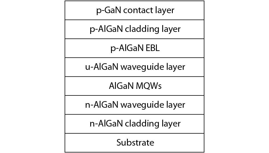
    In recent years, because of their small size, high efficiency and environment-friendly advantages, III-nitride based ultraviolet (UV) light-emitting diodes (LEDs) have been widely used in many areas to substitute for mercury lamps, such as in 3D printing, curing and sterilization. III-nitride alloys cover the whole UV spectrum which is comprised of UV-A (320–400 nm), UV-B (280–320 nm) and UV-C (200–280 nm) by controlling Al/Ga/In content. In addition, III-nitride based UV laser diodes (LDs) also have some potential applications in the case of high-power-density, narrow-spectrum, good-directional lighting. However, III-nitride based UV laser diodes still have many challenges such as poor crystal quality and low hole concentration in p-type AlGaN.

    The typical epitaxial layer structure of AlGaN-based UV LDs is shown in Fig. 1, including cladding layer (CL), waveguide layer (WG), multiple quantum wells (MQWs), electron blocking layer (EBL) and contact layer. Thick cladding layer is necessary to confine the light in the active layer. Therefore, strain controlling layer is also important because there is large strain between AlGaN and GaN or AlN. Usually, Al content of cladding layer is about 10% larger than that of WG which is equal to Al content of barrier layer in MQWs. Because UV LDs are always pumped and excited under high current density, a higher crystal quality and higher hole concentration in p-type layers are necessary for them than for LEDs. The design of MQWs of LDs should also conform the injection with high current density, which is much different from LEDs.

    Typical epitaxial layer structure of AlGaN-based UV laser diodes.

    Figure 1.Typical epitaxial layer structure of AlGaN-based UV laser diodes.

    In 1997, Nakamura et al. in Nichia Corporation achieved the first long-lifetime InGaN UV LD in the world. The laser emission wavelength is 395 nm under room temperature (RT) continuous-wave (cw) operation, with currents of 60 mA and the lifetime is longer than 1150 h[1]. In this work, they used an epitaxially laterally overgrown (ELOG) GaN template to reduce the number of threading dislocations of GaN epilayer. GaN/Al0.14Ga0.86N modulation-doped strained-layer superlattices (MD-SLSs) was used as cladding layer instead of thick AlGaN layers in order to prevent the formation of cracks and dislocations due to the lattice mismatch and improve the hole concentration of p-type cladding layer. High-reflection facet coatings (50%) consisting of two pairs of quarter-wave TiO2/SiO2 dielectric multilayers were used to reduce the threshold current.

    Based on these technologies, Nagahama et al. in Nichia Corporation first achieved the single GaN quantum well UV laser diode[2] and AlxInyGa(1–xy)N quantum well UV laser diode[3] in 2001. The emission wavelength of GaN UV laser was shorten to 366.9 nm and the threshold current density and voltage of this LD were 3.5 kA/cm2 and 4.6 V under 25 °C cw operation. The estimated lifetime was approximately 2000 h at an output power of 2 mW. In this work, InGaN layer was used for relaxing tensile strain in the AlGaN MD-SLS cladding layer possibly by bringing new threading dislocations from InGaN layers. AlxInyGa(1–xy)N quantum well was used to reduce quantum confined Stark effect (QCSE) and increase the local state effect instead of GaN well layer. However, the lifetime became 500 h, much shorter than GaN well UV LD possibly due to the poor quality of Alx InyGa(1–xy)N well. In 2003, Masui et al. in the same corporation improved the lifetime of 365 nm AlxInyGa(1–xy)N quantum well UV LD to approximately 2000 h at an output power of 3 mW under cw operation at 30 °C by using GaN substrate[4]. At the same time, they shorten the emission wavelength of UV LD to 354.7 nm under pulse current injection at 25 °C.

    In 2004, Amano and Akasaki group in Meijo University reported the 350.9 nm UV LD grown on thick, crack-free, low-dislocation density AlGaN grown by the combination of heteroepitaxial lateral overgrowth (HELO) and LT interlayer[5]. The HELO can reduce the strain and dislocation density of AlGaN cladding layer. Then, in 2008, Yoshida et al. reduced the wavelength of UV LD to 342 nm and 336 nm by hetero-FACELO method[6, 7]. In addition, Zhao et al. realized the UV LDs in China[8].

    Some groups did many researches for UV-B and UV-C LDs. However, it is very difficult to achieve the electric-injection emission partly due to low hole concentration in p-type high-Al AlGaN cladding layer[9]. Recently, Amano group and Asashi-kasei corporation cooperated to achieve the 271.8 nm UV LD, the first UV-C electrically injected LD in the world[10]. In this work, they used distributed polarization doping (DPD) approach to achieve high hole concentration in p-type cladding layer which serves simultaneously as the electron blocking layer. In addition, they used low dislocation density AlN substrate to improve the crystal quality of each layer. This work should be a milestone in the development of UV LDs.

    The low-dislocation-density GaN or AlN substrate is necessary to use for UV LDs due to high crystal quality. DPD or short period superlattice (SPSL) will be used to solve the problem of preparing p-type cladding layer. The design of strain-controlling layer is also important at the same time. In the future, many challenges of III-nitride based UV LDs need to be solved. The III-nitride based UV LDs are expected to replace the mercury lamp and be widely used in human society.

    References

    [1] S Nakamura, h M Senoh, a S Nagahama et al. InGaN/GaN/AlGaN-based laser diodes with modulation-doped strained-layer superlattices grown on an epitaxially laterally overgrown GaN substrate. Appl Phys Lett, 72, 211(1998).

    [2] S Nagahama, o T Yanamoto, o M Sano et al. Ultraviolet GaN single quantum well laser diodes. Jpn J Appl Phys, 40, L785(2001).

    [3] S Nagahama, o T Yanamoto, o M Sano et al. Characteristics of ultraviolet laser diodes composed of quaternary AlxInyGa(1–xy)N. Jpn J Appl Phys,, 40, L788(2001).

    [4] S Masui, a Y Matsuyama, o T Yanamoto et al. 365 nm ultraviolet laser diodes composed of quaternary AlInGaN alloy. Jpn J Appl Phys, 42, L 1318(2003).

    [5] K Iida, a T Kawashima, i A Miyazaki et al. 350.9 nm UV laser diode grown on low-dislocation-density AlGaN. Jpn J Appl Phys, 43, L499(2004).

    [6] H Yoshida, a Y Yamashita, a M Kuwabara et al. A 342-nm ultraviolet AlGaN multiple-quantum-well laser diode. Nat Photonics, 2, 551(2008).

    [7] H Yoshida, Y Yamashita, a M Kuwabara et al. Demonstration of an ultraviolet 336 nm AlGaN multiple-quantum-well laser diode. Appl Phys Lett, 93, 241106(2008).

    [8] D G Zhao, g J Yang, u Z S Liu et al. Fabrication of room temperature continuous-wave operation GaN-based ultraviolet laser diodes. J Semicond, 38, 051001(2017).

    [9] D B Li, g K Jiang, n X J Sun et al. AlGaN photonics: recent advances in materials and ultraviolet devices. Adv Opt Photonics, 10, 43(2018).

    [10] Z Y Zhang, o M Kushimoto, i T Sakai et al. A 271.8 nm deep-ultraviolet laser diode for room temperature operation. Appl Phys Express, 12, 124003(2019).