
A. Menani, L. Dehimi, S. Dehimi, F. Pezzimenti. Modelling and optical response of a compressive-strained AlGaN/GaN quantum well laser diode[J]. Journal of Semiconductors, 2020, 41(6): 062301
- Journal of Semiconductors
- Vol. 41, Issue 6, 062301 (2020)
Abstract
1. Introduction
In the last few decades, gallium arsenide (GaAs) alloys and III–V semiconductors were the most commercialized materials for laser diodes (LDs)[
An important challenge in the field of optoelectronics is the development of short wavelength lasers which can emit coherent light in green, blue, violet, and ultraviolet (UV) regimes. In particular, III-nitride and IV wide bandgap materials have received a great attention for the promising realization of several devices[
In this paper, the optical gain and threshold current density of a compressive-strained AlGaN/GaN quantum well (QW) laser, which emits in the UV regime, have been investigated in a wide range of temperatures by means of the Atlas-Silvaco physical device simulator. The optical gain spectra have been calculated by using a simple parabolic band model and also a multiband formalism based on the perturbation theory (k.p model) that is particularly suited for crystals with wurtzite symmetry. In the first case, we have assumed the electron and hole wavefunctions calculated by taking into account transitions that occur only between the first levels of the conduction band and valence band (band-to-band model) similarly to Ref. [35]. In the second case, we have considered the intervalence band absorption effects from different energy levels, namely heavy-hole (HH), light-hole (LH), and split-off (SO), computed via a 6 × 6 k.p model in the QW region[
2. Calculation models and parameters
For a single QW with a width Lw, the threshold current density can be written as[
The optical gain can be defined as the fractional increase in photons per unit of length in response to a given photon flux[
where ε0 is the free-space dielectric constant, nr is the material refractive index, h is Planck's constant, c is the light velocity, e is the electron charge, E is the transition energy, Im,n is the overlap integral of electron and hole wavefunctions, Γ is the line-width due to Lorentzian broadening, Lw is the well width, Mb is the polarization-dependent bulk momentum matrix element, m0 is the carrier mass in free-space, and mr = (mc−1 + mv−1)−1 is the reduced effective mass which depends on the valence (mv) and conduction (mc) band effective masses. Finally, in Eq. (1), the sum is taken all over the transitions between the electron and hole subband energy levels, labelled in the following as En and Em, and the Fermi-Dirac distribution functions fnc and fmv are described by using
where nth and τth are the threshold carrier density and lifetime, respectively. By increasing the temperature, the intrinsic losses of the laser diode tend to increase while the device internal efficiency factor tends to decrease. The variation of the threshold current with temperature is assumed in the form[
where Jth is the reference value at a given temperature, and T0 is a specific parameter that determines the effective degradation of the diode conduction capabilities and therefore the resulting increase of the laser threshold current. This temperature parameter was calculated for AlGaN-based laser diodes by fitting experimental data on Jth in Ref. [14]. In particular, T0 was estimated to be 132 K in the low temperature range and it drops down to 89 K for T higher than about 395 K.
where Emn = En − Em, and EFc and EFv are the electron and hole quasi-Fermi levels, respectively. To calculate the optical gain, therefore, we have to calculate the QW subband energies and the relative electron and hole wavefunctions in the device active region, namely the GaN layer situated between the two AlGaN barrier layers. The strain effect and the strong built-in field effect due to the piezoelectric polarization of III-nitride materials have been carefully taken into account in the calculations of the laser optical gain.
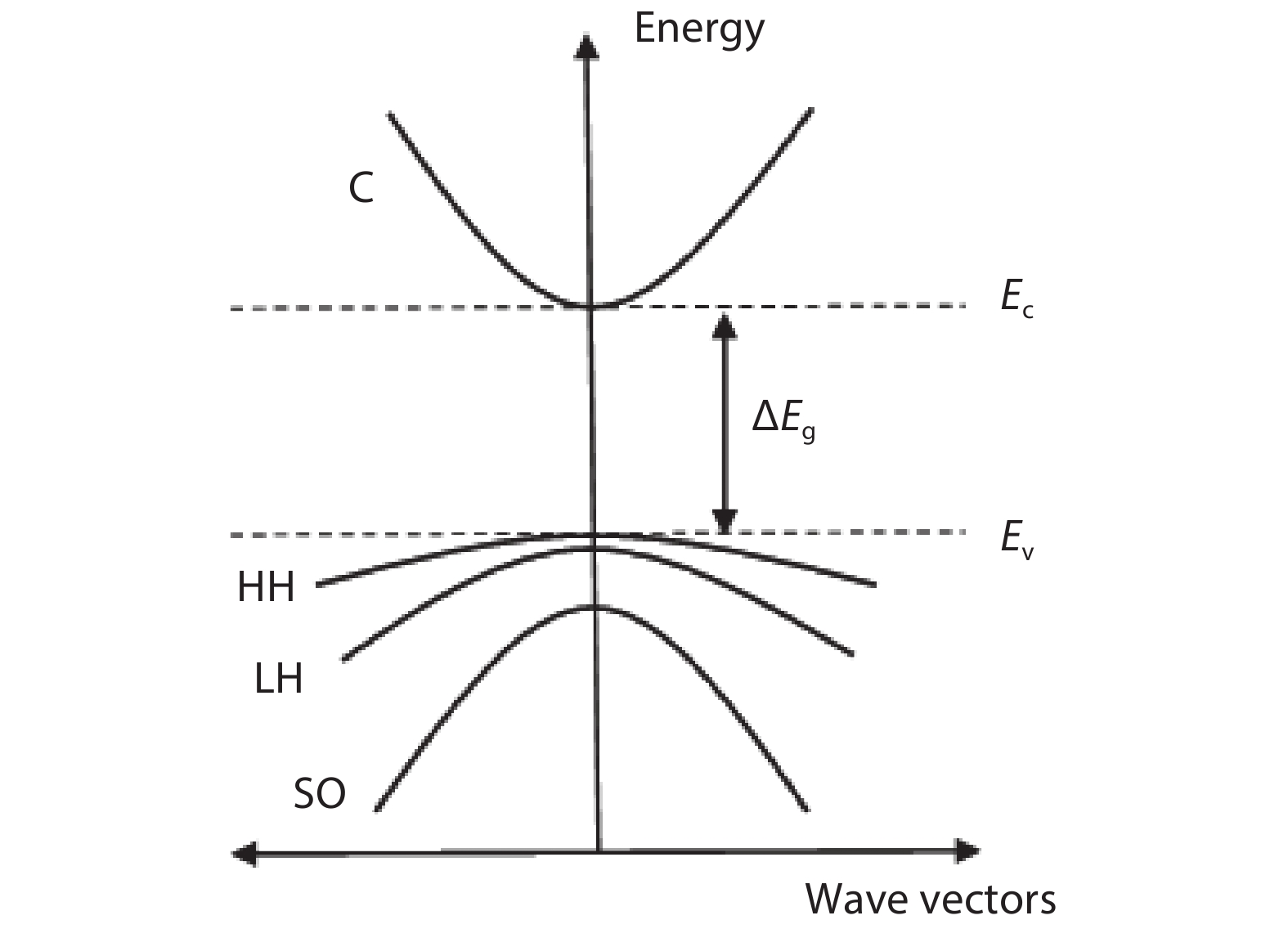
A schematic diagram of the energy band structure assumed for modelling and simulations is shown in Fig. 1.
![]()
Figure 1.Schematic diagram showing the energy band states in the QW: conduction (C), heavy-hole (HH), light-hole (LH), and split-off (SO).
By using the perturbation theory in considering the valence intersubband transitions, the hole energy states have been computed via a 6 × 6 diagonalized k.p Hamiltonian matrix in the form of[
where
These matrix elements, which contain the general expressions for a strained semiconductor, can be expressed as follows:
where A1–6 are hole effective mass parameters, Δ1–3 are split energies, D1–4 are shear deformation potentials, kt and kz are wave vectors along the device x–y basal plane and z-direction, respectively. In addition, the strain tensors relative to the lattice constant mismatch between the QW and barrier layers, i.e. εxx, εyy, and εzz, are modelled through the expressions:
where ai and ci are lattice constants in the device structure.
The polarization modelling includes both the spontaneous polarization (Psp), which is strain independent, and the piezoelectric polarization along the growth direction <0001> given by [
where the terms Cij are elastic constants and dpz is an opportune coefficient.
The reference parameters of the binary compounds GaN and AlN (wurtzite crystals) are summarized in Table 1[
In addition, for a specific AlxGa1–xN ternary alloy, the variation of Eg due to the effective Al molar fraction x was calculated by using[
where the so-called bowing parameter fixed to 0.6 accounts for the deviation from a linear interpolation between the values of EgAlN(T) and EgGaN(T) calculated by considering that the coefficients α and β are also dependent on x as follows:
Finally, Adachi's refractive index model aids to calculate the AlxGa1–xN x-dependent refractive index as[
where the material parameters A and B are in the form
3. Results and discussion
The investigated device structure consists of a GaN active layer situated between two 80-nm-thick AlxGa1–xN barrier regions. By fixing x = 0.1 and Lw = 40 Å as entry data for simulations, the optical gain spectrum is firstly calculated as a function of the wavelength for different carrier densities in the range 1 × 10¹⁸–1 × 1019 cm–3 as shown in Fig. 2. The value n = 1 × 1018 cm–3 can, in fact, be assumed as the threshold carrier density (transparency density) for the considered device. As we can see, the increase of the injection level in the active region determines the increase of the maximum optical gain for both the band-to-band and 6-band k.p models. These behaviours are due to the filling of high states in the conduction band and valence band with the resulting increase of the emission phenomena as reported for similar laser structures[
![]()
Figure 2.(Color online) Optical gain spectrum in an Al0.1Ga0.9N/GaN/Al0.1Ga0.9N QW laser as a function of the wavelength for different carrier densities in the active region at
The curves in Figs. 2(a) and 2(b) are, however, quite different each other. In fact, the optical gain values in Fig. 2(b) are strongly increased if compared to those reported in Fig. 2(a) as a consequence of the intermixing of available states in the valence subbands. In addition, the gain spectrum calculated using the band-to-band model is rather wide as a consequence of the large energy difference between the quasi-Fermi levels which results from the model assumptions.
The optical gain dependence on the Al molar fraction for n = 1 × 1019 cm–3 is shown in Fig. 3.
![]()
Figure 3.(Color online) Optical gain spectrum as a function of the Al molar fraction at
It is worth noting that in AlxGa1–xN/GaN QW lasers an increasing value of x meaningfully increases the maximum optical gain moving the gain spectrum towards the shorter wavelengths. This shift is due to the increase of the AlxGa1–xN bandgap, calculated as wide as 3.896 eV for x = 0.2, and the change of the quantization energy. At the same time, the increase of the maximum gain value is mainly due to the increase in the optical confinement because the refractive index of the barrier layers tends to become higher than that in the GaN active region.
A fundamental geometrical parameter in the design of the considered device is the width of the GaN well (Lw). The plot of the maximum optical gain calculated for different values of Lw in the range 30 to 60 Å is shown in Fig. 4. A wider QW penalizes increasingly the optical gain and Lw = 40 Å should be assumed as a limit value in this study. The wider the QW, the stronger electrons and holes are separated by the piezoelectric field and therefore the optical gain reduces. In other words, when the QW width increases, the density of states in this region decreases.
![]()
Figure 4.(Color online) Optical gain spectrum as a function of the GaN QW width (
The temperature effects on the optical gain behaviour are shown in Fig. 5. Here, it is evident that the temperature has only a limited impact on the maximum gain value. In more detail, the optical gain tends to decrease as the temperature increase in accordance with the variation of the Fermi-Dirac distributions in Eqs. (2) and (3). Meanwhile, by increasing the temperature, the GaN bandgap shrinks and carriers can scatter to other subbands leading to a change of the spectrum range that tends to shift toward the lower photon energies.
![]()
Figure 5.(Color online) Dependence of the optical gain on temperature (
The temperature-dependent GaN bandgap profile is shown in Fig. 6. The interatomic spacing increases when the amplitude of the atomic vibrations increases due to an increased thermal energy. This effect causes a dilatation of the lattice and leads to a displacement of the conduction and valence band edges.
![]()
Figure 6.(Color online) GaN bandgap energy as a function of the temperature.
Finally, the laser threshold current density variation with temperature in the range 260–340 K is shown in Fig. 7.
![]()
Figure 7.(Color online) Threshold current density dependence on temperature (
By using the k.p model, the increase of the threshold current density with temperature is stronger than the simple band-to-band behaviour. This increase is on the order of a factor 5 at T = 340 K. The minimum Jth value is around 60 A/cm2 for both models at very low temperatures.
4. Conclusion
In this paper, we have investigated the optical response of a strained wurtzite GaN/AlxGa1–xN quantum well laser. The effects of the carrier density, quantum well width, Al concentration in the barrier layers, and temperature have been taken into account by using two different band energy models in the device structure. In particular, the optical gain increases by increasing the carrier density as well as the Al concentration whereas it decreases with the quantum well width and temperature. The simulation analysis based on the k.p model, with a more accurate calculation, provides better results in terms of optical gain reducing also the dependence of the threshold current density on temperature. Our analysis suggests that laser diodes based on a GaN/AlGaN QW can emit in the UV with a significant optical gain and a low threshold current density.
References
[1]
[2]
[3] C Kieleck, n M Eichhorn, h A Hirth et al. High-efficiency 20–50 kHz mid-infrared orientation-patterned GaAs optical parametric oscillator pumped by a 2
[4] H C Liu, R Dudek, A Shen et al. High absorption quantum-well infrared photodetectors. Appl Phys Lett, 79, 4237(2001).
[5] F Bouzid, F Pezzimenti, L Dehimi et al. Analytical modeling of dual-junction tandem solar cells based on an InGaP/GaAs heterojunction stacked on a Ge substrate. J Electron Mater, 48, 4107(2019).
[6] V M Ustinov, A E Zhukov. GaAs-based long-wavelength lasers. Semicond Sci Technol, 15, R41(2000).
[7] A Rogalski. Infrared detectors: an overview. Infrared Phys Tech, 43, 187(2002).
[8] J Justice, C Bower, M Meitl et al. Wafer-scale integration of group III–V lasers on silicon using transfer printing of epitaxial layers. Nat Photonics, 6, 610(2012).
[9] F Bouzid, L Dehimi, F Pezzimenti et al. Numerical simulation study of a high efficient AlGaN-based ultraviolet photodetector. Superlattice Microstruct, 122, 57(2018).
[10] S Dehimi, L Dehimi, A Aissat. Study and Simulation of a quantum well structure based ZnTe/Zn
[11] H Liu, T Wang, g Q Jiang et al. Long-wavelength InAs/GaAs quantum-dot laser diode monolithically grown on Ge substrate. Nat Photonics, 5, 416(2011).
[12] F G Della Corte, G De Martino, F Pezzimenti et al. Numerical simulation study of a low breakdown voltage 4H-SiC MOSFET for photovoltaic module-level applications. IEEE Trans Electron Devices, 65, 3352(2018).
[13]
[14] H Yoshida, M Kuwabara, Y Yamashita et al. AlGaN-based laser diodes for the short-wavelength ultraviolet region. New J Phys, 11, 125013(2009).
[15] F Bouzid, L Dehimi, F Pezzimenti. Performance analysis of a Pt/n-GaN Schottky barrier UV detector. J Electron Mater, 46, 6563(2017).
[16] S P DenBaars, D Feezell, K Kelchner et al. Development of gallium-nitride-based light-emitting diodes (LEDs) and laser diodes for energy-efficient lighting and displays. Acta Mater, 61, 945(2013).
[17] Y Marouf, L Dehimi, F Pezzimenti. Simulation study for the current matching optimization in In0.48Ga0.52N/In0.74Ga0.26N dual junction solar cells. Superlattice Microstruct, 130, 377(2019).
[18] H Bencherif, L Dehimi, F Pezzimenti et al. Improving the efficiency of a-Si: H/c-Si thin heterojunction solar cells by using both antireflection coating engineering and diffraction grating. Optik, 182, 682(2019).
[19] K Zeghdar, L Dehimi, F F Pezzimenti et al. Simulation and analysis of the current-voltage-temperature characteristics of Al/Ti/4H-SiC Schottky barrier diodes. Jpn J Appl Phys, 58, 014002(2019).
[20] A Fritah, L Dehimi, F Pezzimenti et al. Analysis of
[21] R M Farrell, D A Haeger, P S Hsu et al. High-power blue-violet AlGaN-cladding-free m-plane InGaN/GaN laser diodes. Appl Phys Lett, 99, 171113(2011).
[22] F Bouzid, F Pezzimenti, L Dehimi et al. Numerical simulations of the electrical transport characteristics of a Pt/n-GaN Schottky diode. Jpn J Appl Phys, 56, 094301(2017).
[23] H Bencherif, L L Dehimi, F Pezzimenti et al. Analytical model for the light trapping effect on ZnO: Al/c-Si/SiGe/c-Si solar cells with an optimized design. Proc International Conference on Applied Smart Systems – ICASS(2018).
[24] Y Marouf, L Dehimi, F Bouzid et al. Theoretical design and performance of In
[25] E Monroy, F Guillot, S Leconte et al. III-nitride nanostructures for infrared optoelectronics. Acta Phys Pol A, 110, 295(2006).
[26] S Rao, G Pangallo, F Pezzimenti et al. High-performance temperature sensor based on 4H-SiC Schottky diodes. IEEE Electron Device Lett, 36, 720(2015).
[27] G De Martino, F Pezzimenti, F G Della Corte. Interface trap effects in the design of a 4H-SiC MOSFET for low voltage applications. Proc International Semiconductor Conference – CAS(2018).
[28] H Bencherif, L Dehimi, F Pezzimenti et al. Temperature and SiO2/4H-SiC interface trap effects on the electrical characteristics of low breakdown voltage MOSFETs. Appl Phys A, 125, 294(2019).
[29] M L Megherbi, F Pezzimenti, L Dehimi et al. Analysis of different forward current-voltage behaviours of Al implanted 4H-SiC vertical p–i–n diodes. Solid-State Electron, 109, 12(2015).
[30] H Bencherif, L Dehimi, F Pezzimenti et al. Multiobjective optimization of design of 4H-SiC power MOSFETs for specific applications. J Electron Mater, 48, 3871(2019).
[31] M Ikeda, T Mizuno, M Takeya et al. High-power GaN-based semiconductor lasers. Phys Status Solidi, 6, 1461(2004).
[32] F Pezzimenti, H Bencherif, A Yousfi et al. Current–voltage analytical model and multiobjective optimization of design of a short channel gate-all-around-junctionless MOSFET. Solid-State Electron, 161, 107642(2019).
[33] A Asgari, S Dashti. Optimization of optical gain in Al
[34] E F Schubert, J K Kim. Solid-state light sources getting smart. Science, 308, 1274(2005).
[35] T Ohtoshi, K Yamaguchi, C Nagaoka et al. A two dimensional device simulator of semiconductor lasers. Solid-State Electron, 30, 627(1987).
[36] S L Chuang, C S Chang. k.p method for strained wurtzite semiconductors. Phys Rev B, 54, 2491(1996).
[37] S L Chuang. Optical gain of strained wurtzite GaN quantum-well lasers. IEEE J Quantum Electron, 32, 1791(1996).
[38] TCAD Silvaco. Atlas user’s manual device simulation software. California: Silvaco Int.(2016).
[39] F Bernardini, V Fiorentini. Spontaneous versus piezoelectric polarization in III–V Nitrides: Conceptual aspects and practical consequences. Phys Status Solidi B, 216, 391(1999).
[40] O Ambacher, J Majewski, C Miskys et al. Pyroelectric properties of Al(In)GaN/GaN heteroand quantum well structures. J Phys Condens Mat, 14, 3399(2002).
[41]
[42] N Nepal, J Li, M L Nakarmi et al. Temperature and compositional dependence of AlGaN the energy band gap of alloys. Appl Phys Lett, 87, 242104(2005).
[43] H Dakhlaoui. Linear and nonlinear optical absorption coefficients and refractive index changes in GaN/Al
[44] S Dehimi, L Dehimi, T Asar et al. Modelling of a Cd1–
[45]
[46] S Dehimi, L Dehimi, T Asar et al. Modeling and simulation of Zn
[47] S Dehimi, A Aissat, D Haddad et al. Optimization of optical gain in In
[48] A Aissat, S Nacer, F Ykhlef et al. Modeling of Ga1−

Set citation alerts for the article
Please enter your email address
© Copyright 2018-2021 | Chinese Laser Press. All Rights Reserved 沪ICP备15018463号-20