• Photonics Research
  • Vol. 5, Issue 6, 654 (2017)
Mahmoud H. Elshorbagy1、2, Alexander Cuadrado1, and Javier Alda1、*
Author Affiliations
  • 1Optics Department, University Complutense of Madrid, Faculty of Optics and Optometry, Av. Arcos de Jalon, 118, 28037 Madrid, Spain
  • 2Physics Department, Faculty of Science, Minia University, University Campus, 61519 El-Minya, Egypt
  • show less
    DOI: 10.1364/PRJ.5.000654 Cite this Article Set citation alerts
    Mahmoud H. Elshorbagy, Alexander Cuadrado, Javier Alda. High-sensitivity integrated devices based on surface plasmon resonance for sensing applications[J]. Photonics Research, 2017, 5(6): 654 Copy Citation Text show less
    (a) Classic Kretschmann configuration with a glass prism coated with a gold thin film in contact with the analyte. The SPR is generated at the metal/analyte interface. (b) 2D cross section of the unit cell of an array of long-wire slot antennas (nanoslits) that generates SPR interacting with the analyte. The system is deposited on a glass substrate as a nanostructure metal layer, M1, a dielectric buffer layer, BL, and a final second metallic layer, M2. The SPR happens at the M2/analyte interface.
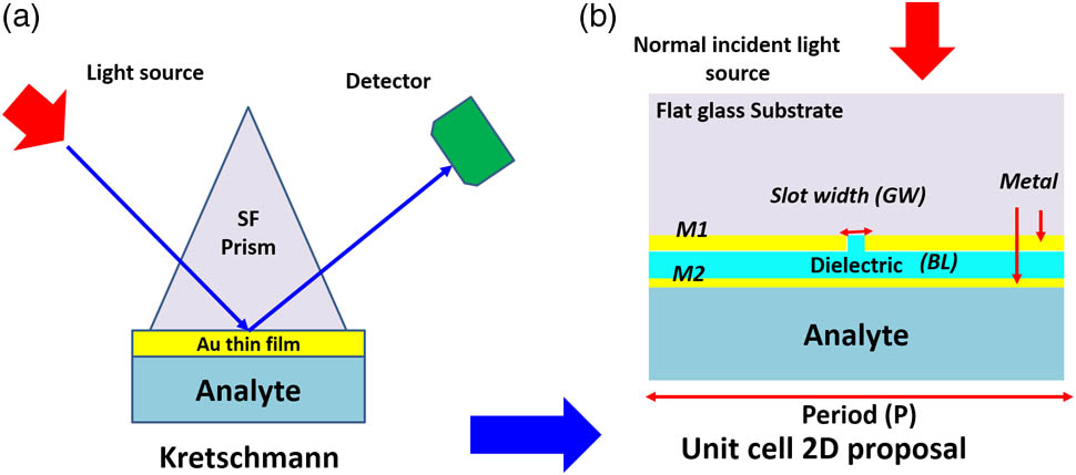
    Fig. 1. (a) Classic Kretschmann configuration with a glass prism coated with a gold thin film in contact with the analyte. The SPR is generated at the metal/analyte interface. (b) 2D cross section of the unit cell of an array of long-wire slot antennas (nanoslits) that generates SPR interacting with the analyte. The system is deposited on a glass substrate as a nanostructure metal layer, M1, a dielectric buffer layer, BL, and a final second metallic layer, M2. The SPR happens at the M2/analyte interface.
    (a) Spectral response of the device showing three reflectance dips: SPRM2 appears at the M2/analyte interface, SPRM1 appears at the substrate/M1 interface and is not accessible in this design, and a guided mode that corresponds to light trapped within the buffer layer. (b) Magnetic field maps at the wavelengths where the three minima of the reflectance occur.
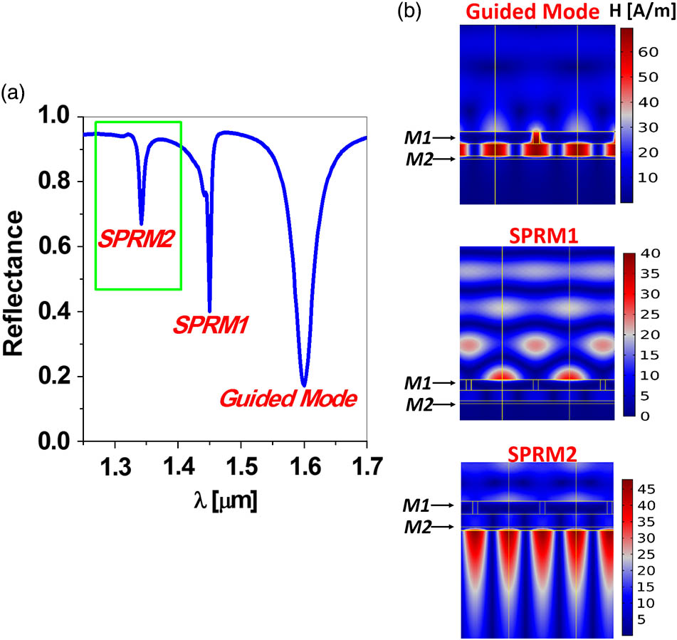
    Fig. 2. (a) Spectral response of the device showing three reflectance dips: SPRM2 appears at the M2/analyte interface, SPRM1 appears at the substrate/M1 interface and is not accessible in this design, and a guided mode that corresponds to light trapped within the buffer layer. (b) Magnetic field maps at the wavelengths where the three minima of the reflectance occur.
    Left column shows the spectral reflectance for various cases where the thicknesses, tBL, tM1, and tM2, and the slit width, wG, change (a, c, e, and g respectively). The right column plots in a double-axis representations of the FE (black dots, left axis) and FWHM (blue solid line, right axis) performance parameter functions of the same geometrical dimensions in the same order (b, d, f, and h). The yellow arrows indicate the selected optimum value.
    Fig. 3. Left column shows the spectral reflectance for various cases where the thicknesses, tBL, tM1, and tM2, and the slit width, wG, change (a, c, e, and g respectively). The right column plots in a double-axis representations of the FE (black dots, left axis) and FWHM (blue solid line, right axis) performance parameter functions of the same geometrical dimensions in the same order (b, d, f, and h). The yellow arrows indicate the selected optimum value.
    (a) Spectral reflectances for three values of the period, P. It shows the overall shift caused by the variation of the period. (b) Amplitude of the magnetic field along the structure at the resonance wavelength.
    Fig. 4. (a) Spectral reflectances for three values of the period, P. It shows the overall shift caused by the variation of the period. (b) Amplitude of the magnetic field along the structure at the resonance wavelength.
    Effect of substrate material on the spectral response. This response shifts when changing the index of refraction of the analyte, na, but the shape of the spectral reflectance remains the same. The solid lines are for na=1.33 and the dashed lines are for na=1.34.
    Fig. 5. Effect of substrate material on the spectral response. This response shifts when changing the index of refraction of the analyte, na, but the shape of the spectral reflectance remains the same. The solid lines are for na=1.33 and the dashed lines are for na=1.34.
    (a) Spectral reflectivity for four different choices of the BL material (MgF2, SiO2, PMMA, and AZO). (b) Dependences of FE and FWHM functions of the index of refraction of the possible choices for the material of the buffer layer. The dashed vertical lines correspond to the index of refraction of the buffer layer material.
    Fig. 6. (a) Spectral reflectivity for four different choices of the BL material (MgF2, SiO2, PMMA, and AZO). (b) Dependences of FE and FWHM functions of the index of refraction of the possible choices for the material of the buffer layer. The dashed vertical lines correspond to the index of refraction of the buffer layer material.
    (a) Effect of different metal combinations for M1 and M2 on the spectral response. We have considered Au, Ag, and Al. (b) Effect of the double-metal layers for M2 on the spectral response. The numbers represent the thicknesses of the two metals Ag–Au in the bimetallic layer. The arrows indicate the preferred choice.
    Fig. 7. (a) Effect of different metal combinations for M1 and M2 on the spectral response. We have considered Au, Ag, and Al. (b) Effect of the double-metal layers for M2 on the spectral response. The numbers represent the thicknesses of the two metals Ag–Au in the bimetallic layer. The arrows indicate the preferred choice.
    Effect of the refractive index of the analyte on the SPR spectral position: (a) for M2 made of a single layer of Ag and (b) for M2 made of a double-metal layer Ag/Au (25/5 nm). (c) Sensitivity (black dotted line, left axis) and (d) FOM (blue solid line, right axis) corresponding to both options for the M2 layer (single metal, Ag, and double metal, Ag–Au, respectively).
    Fig. 8. Effect of the refractive index of the analyte on the SPR spectral position: (a) for M2 made of a single layer of Ag and (b) for M2 made of a double-metal layer Ag/Au (25/5 nm). (c) Sensitivity (black dotted line, left axis) and (d) FOM (blue solid line, right axis) corresponding to both options for the M2 layer (single metal, Ag, and double metal, Ag–Au, respectively).
    Mahmoud H. Elshorbagy, Alexander Cuadrado, Javier Alda. High-sensitivity integrated devices based on surface plasmon resonance for sensing applications[J]. Photonics Research, 2017, 5(6): 654
    Download Citation