Mahmoud H. Elshorbagy, Alexander Cuadrado, Javier Alda, "High-sensitivity integrated devices based on surface plasmon resonance for sensing applications," Photonics Res. 5, 654 (2017)
Copy Citation Text
A metallic nanostructured array that scatters radiation toward a thin metallic layer generates surface plasmon resonances for normally incident light. The location of the minimum of the spectral reflectivity serves to detect changes in the index of refraction of the medium under analysis. The normal incidence operation eases its integration with optical fibers. The geometry of the arrangement and the material selection are changed to optimize some performance parameters as sensitivity, figure of merit, field enhancement, and spectral width. This optimization takes into account the feasibility of the fabrication. The evaluated results of sensitivity (1020 nm/RIU) and figure of merit (614 RIU?1) are competitive with those previously reported.
Optical sensors for the detection and identification of biomolecules and chemical specimens have been developed with increased sensitivity and specificity. Those based on surface plasmon resonance (SPR) [1] have been proposed to beat the limitations in operation and performance of other optical detection approaches, such as ellipsometry [2], interferometry [3], spectroscopy of guided modes in optical waveguide structures [4,5], and some other techniques. SPR can be excited at the interface between a metal and a dielectric when light is incident from the metal side, complying with the wavevector matching conditions [1]. These conditions are fulfilled using a variety of geometrical and material configurations [6]. Among them, we can mention the use of buffer layers [7–9], nanoparticles [10–13], or by coupling to a grating located at the interface [14–17].
The surface plasmon wave decays in the dielectric medium after the metal/dielectric interface where the SPR is generated. This evanescent wave is greatly altered by any change in the refractive index of that dielectric medium. This is the basic principle for the operation of SPR-based sensors relying in refractometric sensing [5]. A common way of generating SPR uses oblique incidence, where the angle of incidence obeys . However, to improve performance, is usually large and depends on the structure of the device, materials, and operating wavelengths. The scientific literature is full of contributions scrutinizing the advantages and limitations of the classical Kretschmann setup. The study by Huang et al.[18] contains a comprehensive analysis of how the performance of the device is strongly dependent on geometry and materials. As a general conclusion, it establishes that by decreasing the refractive index of the substrate (prism) the sensitivity of the device increases. However, this strategy reduces the detection range because it is necessary to move to conditions involving very large angles of incidence.
Besides the Kretschmann configuration, it is also possible to generate SPR using normally incident light. To do that, the use of nanogrooves located at the analyte side has been proposed [19]. It requires slit widths of around 3–12 nm, making the fabrication quite demanding. A similar approach is considered by nanostructuring the top surface of the metal, creating nanocavities on it with a lateral size of about 13 nm [20]. These ideas have been reported and some optimization has been done maximizing the electric field available for an optical interrogation. The remote excitation of SPR using a metallic grating embedded in a dielectric substrate was demonstrated by Lee and Gray [21]. In that paper, the system was optimized in terms of the field enhancements (FEs) and shows how the structure provides narrow bands with high FEs, which could be used for sensing applications. A design of a plasmonic sensor based on the excitation of SPR using a dielectric grating was reported [22]. These sensor strategies account for a sensitivity of about 150 nm/RIU [22], which is considered as moderate and comparable to those using Kretschmann configurations. Sensitivity is an important parameter used to compare optical sensors. This is given as the change in the sensor signal (for example, the location of a minimum or maximum reflectance in terms of the angle of incidence or wavelength) with respect to the change in the measured quantity (index of refraction, temperature, concentration, pressure, etc.). Some previous papers have also reported the use of a nanostructured metallic layer placed on a dielectric/metallic thin-film configuration for plasmonic sensing and interferometry [23–25]. The proposals benefit from the variations in absorption (or reflection) caused by the nanostructured layer that works as a perfect absorber, depending on the index of refraction of the medium under test. These structures are alternatives to the classical Kretschmann setup, allowing spectral interrogation under normal incidence conditions. Plasmonic sensors provide a reasonable value of sensitivity that is limited by constraints related to the geometry; for example, a large angle of incidence increases sensitivity at a cost of a narrow detection range [18,26–29]. Also, material constraints are at play and require biocompatibility, good resistance to oxidation, and chemical stability [30].
Sign up for Photonics Research TOC. Get the latest issue of Photonics Research delivered right to you!Sign up now
In this paper, we propose a periodic array of metallic long-wire slot antenna [31]—an array of nanoslits that scatters the incoming radiation and works under normal incidence conditions. This design can be also seen as a metallic metasurface [32]. The sensed variable is the location of the minimum of the spectral reflectivity. Therefore, we will be interested in knowing how this reflectivity changes with the index of refraction of the medium under analysis. The radiation scattered by the nanostructured layer propagates toward a thin gold film to generate SPR. The proposed device has been optimized to work with competitive sensitivity and figure of merit (FOM). This optimization implies the parameterization of the geometry of the structure: substrate, metallic nanostructured layer, buffer layer, and metal film. Also, an appropriate selection of the material will be considered to improve the spectral response.
The paper is organized as follows. Section 2 describes the geometry and material arrangement of an efficient alternative to the classical Kretschmann configuration that works in normal incidence conditions. The parameters characterizing the performance and driving the optimization of the system are also presented in this section along with the introduction of the simulation tool used in this paper. In Section 3, the geometry is optimized to improve the sensitivity and FOM of the device and how it responds spectrally. After optimizing the geometry, the choice of materials is revised to improve and expand the performance of the system. Section 4 describes an improved proposal that is positively compared with the previous ideas reported in the literature. Finally, Section 5 summarizes the main conclusions of the paper.
2. SENSOR ARRANGEMENT
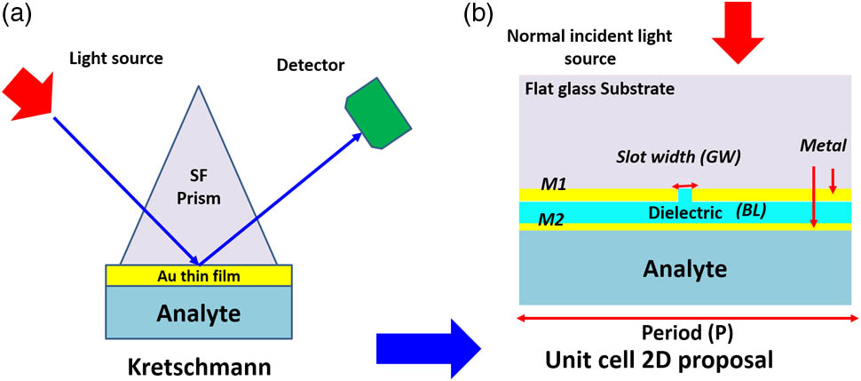
We discuss here a proposal that can be considered as an efficient alternative to the classical Kretschmann configuration [see Fig. 1(a)]. The device is capable of working at normal incidence conditions, allowing its integration, for example, at the end of an optical fiber, attaching the substrate to the end of the fiber, or by setting a collimation optics that is finished by the proposed sensor arrangement fabricated on a glass substrate.
Figure 1.(a) Classic Kretschmann configuration with a glass prism coated with a gold thin film in contact with the analyte. The SPR is generated at the metal/analyte interface. (b) 2D cross section of the unit cell of an array of long-wire slot antennas (nanoslits) that generates SPR interacting with the analyte. The system is deposited on a glass substrate as a nanostructure metal layer, M1, a dielectric buffer layer, BL, and a final second metallic layer, M2. The SPR happens at the M2/analyte interface.
In order to perform the evaluation of the interaction mechanisms involved in the process, we have selected some feasible parameters and materials. The geometry of the sensor is an extruded profile with a 2D cross section that is presented in Fig. 1(b). It consists [from top to bottom in Fig. 1(b)] of a dielectric transparent flat substrate, a nanostructure organized as an array of nanoslits printed on a thin metal film, and a dielectric stand-off layer that is terminated by a very thin metal layer. The analyte, or medium under test, is in contact with this last layer where the SPR propagates and interacts with the analyte.
The material arrangement is deposited on a flat glass substrate made of (optical constants from Ref. [33]). The first metal layer is made of gold (with complex refractive index data obtained from Ref. [34]) having a thickness of . This nanoslit structure has a slit width of , and it is arranged with a spatial period . The role of the nanostructure is to generate a scattering pattern that illuminates a second metal–dielectric interface. After this nanostructure, a dielectric buffer, or stand-off layer, made of (refractive index taken from Ref. [35]) is deposited with a thickness of . can be spin coated [36,37], and the resulting surface is planarized for further deposition. After this stand-off layer, a second metal layer (also made of gold in our first analysis) in the form of a thin film having a thickness of is deposited. After this second metal thin film, we have the medium under test. For simplicity, we used water as the analyte medium. Therefore, we have four material choices (for the two metals, the dielectric buffer layer, and the dielectric substrate), three thicknesses (, , and ), and two more geometrical parameters that define the nanoslit array ( and ).
B. Modeling
A plasmonic sensor using the Kretschmann configuration obeys the following relation [18]: where is the operation wavelength in vacuum, is the refractive index of the prism, is the effective index seen by the plasmon, and is the propagation constant of the surface plasmon excited at an angle of incidence .
In the proposed design, light scatters at the metallic nanostructure and generates a wide range of directions for the propagating vector. This phenomenon can be seen as subwavelength diffraction. The scattered radiation propagates through the dielectric buffer layer toward the second flat metal thin film. Then, an SPR is generated at the metal/analyte interface when light fulfills the following matching condition: where and are the dielectric permitivities of the substrate and analyte media, respectively, and is the real part of the complex dielectric function of the metal thin film M2. The grating diffracts (or scatters) radiation at an angle that is given as where is the diffraction order, and is the period of the nanoslit array. Combining Eqs. (2) and (3), we can derive the condition for SPR generation at the metal/analyte interface [21]:
The same mechanism, but in reflection, originates another SPR resonance at the first metal/substrate interface.
The diffracted light generates the SPR, so the intensity of the SP wave will depend on the diffraction efficiency of the grating; this is the reason for the shallow reflectance dip produced by the structure.
C. Parameterization
The sensitivity of plasmonic devices, , interrogated in reflectance is linked to the change in angle, , or wavelength, , of the minimum of the reflectance of the system when changing the index of refraction, , of the medium under test. In Kretschmann configurations, it is common to express sensitivity as [18]
However, for fiber optics plasmonic sensors, it is better to define sensitivity in terms of a spectral shift: where the subindex , or , defines the parameter used in the interrogation of the system. Alternatively, some operational modes in plasmonic sensors measure the transmittance or the absorption of the device. Although sensitivity, , relates those parameters involved in the operation of the system, it still does not present a full characterization of the performance of the device. This is better expressed as the FOM of the sensor. This parameter is defined as the sensitivity, , divided by the angular, or spectral, full width at half-maximum (FWHM) of the reflectance plot. Using this approach, FOM is expressed as [38]
The goal of the design is to obtain high values of both and FOM.
When optimizing the structure for sensing applications, we are interested in the local FE at the desired location within the medium under test. In this paper, FE will be parameterized as the maximum value of the magnetic field at the sensing interface (metal–analyte) for the SPR wavelength. At the same time, if the system is interrogated spectrally, the width of the spectral resonance, parameterized as the FWHM, should be minimized, allowing higher resolution. Besides, both sensitivity [Eqs. (5) and (6)] and the FOM [Eq. (7)] should be considered to compare the performance of the proposed devices with those already reported in the literature.
D. Simulation
The electromagnetic response has been evaluated using Comsol Multiphysics that has been also used to validate enhancement strategies for the improvement of amorphous Si solar cells [39]. The numerical model has been positively tested by evaluating the response of a Kretschmann configuration device and comparing the computational results with an analytical model of the system [40]. The incoming wavefront is a plane wave with TM polarization and has a magnetic field amplitude of 1 A/m. This numerical analysis reveals three minima of the spectral reflectance of the structure [see Fig. 2(a)], corresponding to three different interactions with the device. The shortest wavelength minimum (SPRM2 in Fig. 2) corresponds with the SPR used for detection that happens at the metal/analyte interface. This interface is flat, allowing easier maintenance and operation. The second minimum (SPRM1 in Fig. 2) appears as an SPR at the metal/substrate interface. The use of SPRM1 would mean an alternative design that requires swapping of the substrate and the analyte and the interaction of the analyte with a nanostructured surface. Additionally, we have checked that an optimization of the performance of a sensor based on the SPRM1 resonance produces lower values in sensitivity and FOM. There exists a third minimum related with a guided mode within the stand-off buffer dielectric layer [39,41]. The magnetic field spatial distributions for the three modes are presented in Fig. 2(b). These maps reinforce the previous explanation of the involved physical mechanisms.
Figure 2.(a) Spectral response of the device showing three reflectance dips: SPRM2 appears at the M2/analyte interface, SPRM1 appears at the substrate/M1 interface and is not accessible in this design, and a guided mode that corresponds to light trapped within the buffer layer. (b) Magnetic field maps at the wavelengths where the three minima of the reflectance occur.
The optimization of the system requires the modification of the geometrical dimensions and an appropriate choice of the materials used for the deposition of the layers. To do that, we may apply a multidimensional optimization of the system where all the available parameters are considered simultaneously. This strategy would need the definition of an optimization merit function [this function cannot be mistaken with the FOM in Eq. (7)]. This optimization function should summarize the performance of the device in terms of characteristic parameters: , FE, FOM, and FWHM (see Subsection 2.C). The definition of this optimization merit function would add an additional variability that could obscure the process. Besides its computational cost, a multidimensional analysis would not provide a clear insight into the effect of a parameter on the response of the device. Because of that, we prefer to perform this optimization taking one parameter at the time and analyzing the influence of this parameter on the variables of interest that summarize the behavior of the system. Therefore, this section contains an optimization procedure for the geometrical parameters of the device, and an analysis of the different choices for the material of the proposed arrangement.
A. Geometry
There are five geometrical parameters that are at play in this device. Three thicknesses (, , and ) and two parameters related with the nanostructure at the first metal layer: the width of the nanoslit and its period ( and , respectively).
The starting point for the optimization process is characterized as follows: substrate ()/metal 1 (Au, )/buffer layer (, )/metal 2 (Au, )/analyte (water). The nanostructure is characterized by the following parameters: and .
The results from this optimization procedure are plotted in Fig. 3. The left column of this figure contains the spectral reflectance when changing the geometrical parameters. The right column represents two performance parameters in terms of the variation of the geometrical parameter under study. We have represented in this column the FE factor expressed as the maximum value of the magnitude of the magnetic field at the analyte medium (black dotted line, left axis) and the FWMH of the spectral reflectance (blue solid line, right axis). The arrows within each plot point to the selected value of the parameter under analysis. At the same time, the rows, from top to bottom, show the effect of changing the geometrical parameters in sequential order: .
Figure 3.Left column shows the spectral reflectance for various cases where the thicknesses, , , and , and the slit width, , change (a, c, e, and g respectively). The right column plots in a double-axis representations of the FE (black dots, left axis) and FWHM (blue solid line, right axis) performance parameter functions of the same geometrical dimensions in the same order (b, d, f, and h). The yellow arrows indicate the selected optimum value.
The first parameter that is considered is the thickness of the buffer layer, . This choice is based in the important role of this layer in the propagation of the scattered radiation coming from the nanostructured first metal layer, M1, and impinging on the second metal layer, M2. Figures 3(a) and 3(b) show how the spectral shape is narrower for and becomes wider and the minimum degrades for thicker values. We can also see that the maximum FE does not coincide with the minimum FWHM but remains at a reasonably high plateau. Although the FE factor degrades as the buffer layer is thicker, those values will increase along the optimization process. When varying [see Figs. 3(c) and 3(d)], there is a clear minimum at . For this value, FE reaches a stable value of around 50 A/m. The thickness of the second metal, , also modifies the spectral reflectance. When this layer is thinner, the minimum in reflectance is shallower, and when the film becomes thicker, the shape is wider, degrading FWHM. Then, a value of is chosen that corresponds with a maximum of the FE parameter.
The last two geometrical parameters of this device play quite different roles. The width of the slit, , determines the angular pattern of the scattered radiation, and the value of the period of the grating changes the spectral and angular location of the grating lobe. When analyzing the width of the individual grooves, we find that a value of is feasible and produces quite a low value of the FWMH with a reasonable value of the FE parameter [see Figs. 3(g) and 3(h)]. Figure 4(a) shows that, by using the period of the pattern, , we can spectrally tune the response to a given specific band, even moving to the visible range. However, the performance of the system is better at the selected near-infrared wavelengths.
Figure 4.(a) Spectral reflectances for three values of the period, . It shows the overall shift caused by the variation of the period. (b) Amplitude of the magnetic field along the structure at the resonance wavelength.
From the previous sequential optimization, we find the following arrangement: substrate ()/metal 1 (Au, )/buffer layer (, )/metal 2 (Au, )/analyte (water). The nanostructure is characterized by the following parameters: and . This structure produces a profile of the amplitude of the magnetic field that is having a maximum at the second metal/analyte interface, where the SPR is generated. Figure 4(b) shows how the SPR amplitude is fitted to an exponential decay function of the form while and are constants, is the coordinate along the direction of propagation, and is the decay length of the SPR wave. The fitting of the model provides a value of , which is directly related with the interaction volume.
B. Materials
In the previous subsection we focused our attention on the effect of the geometry of the different elements and layers of the proposed device. Now we will consider some material options that change the final performance of the system. The first material choice that we consider is for the substrate. Some feasible options arranged from lower to higher index of refraction of the substrate, , are , , and SF glass (optical constants from Ref. [42]). Figure 5 shows how the choice of the substrate does not change the shape of the spectral response very much. However, when considering the change of the spectra in terms of the variation of the index of refraction of the analyte, , we can see how an SF glass substrate produces a slightly larger variation in the spectral location of the peak, meaning a larger value of . This behavior is opposite to that obtained for Kretschmann configurations, where a low-index substrate is preferable to enhance sensitivity. This difference can be explained by the material arrangement of the proposed device, where the buffer layer works as the effective substrate, and will require a low-index material to optimize the device. Both the spectral behavior and the sensitivity of the device are almost independent of the substrate. This is also relevant from an economic point of view because the low-index substrate required by conventional Kretschmann configurations can be replaced by a cheaper substrate.
Figure 5.Effect of substrate material on the spectral response. This response shifts when changing the index of refraction of the analyte, , but the shape of the spectral reflectance remains the same. The solid lines are for and the dashed lines are for .
The previous assumption about the buffer layer is corroborated when analyzing how the response varies when changing the material of this layer. We have considered materials that could be spin coated or casted to fill the nanoslit and generate a flat surface to deposit the last metal layer, M2, on top of it. Our analysis has considered , , poly(methyl methacrylate) PMMA (optical constants from Ref. [43]), and aluminum-doped zinc-oxide AZO (optical constants from Ref. [44]). This layer is of importance because it transfers the scattered radiation from the nanoslits toward the metal/dielectric interface where the SPR is generated. The results from the analysis of the spectral reflectance [see Fig. 6(a)] shows that a low-index material, such as , provides the best results in FE and FWHM [see Fig. 6(b)] and also in and FOM. This figure uses the index of refraction of the material as the parameter to calculate these variables.
Figure 6.(a) Spectral reflectivity for four different choices of the BL material (, , PMMA, and AZO). (b) Dependences of FE and FWHM functions of the index of refraction of the possible choices for the material of the buffer layer. The dashed vertical lines correspond to the index of refraction of the buffer layer material.
Finally, we can consider how the metal selection for the nanostructured layer and the second metal layer may change the performance and applicability of the sensor. The metals commonly used for SPR applications are Au, Ag, and Al (with complex refractive index values from Ref. [34]). The results of this material analysis are given in Fig. 7(a) and show that the narrowest spectrum appears for a nanostructured metal layer made of gold (M1) and a second metal layer of silver (M2).
Figure 7.(a) Effect of different metal combinations for M1 and M2 on the spectral response. We have considered Au, Ag, and Al. (b) Effect of the double-metal layers for M2 on the spectral response. The numbers represent the thicknesses of the two metals Ag–Au in the bimetallic layer. The arrows indicate the preferred choice.
The result of this material optimization produces a device with the following arrangement: substrate (SF Glass)/metal 1 (Au, )/buffer layer (, )/metal 2 (Ag, )/analyte (water), being and .
An additional analysis should take into account the biocompatibility and degradation characteristics of metals, with Au being a better choice when biological samples for water-solvent analysis are considered. A solution to passivize the Ag–analyte layer adds a very thin layer of gold on top of it. The effect of this additional layer is shown in Fig. 7(b), where a double layer of Ag/Au (with thicknesses 25/5 nm, respectively) provides a quite sharp response.
4. RESULTS
From the results obtained in the previous section, it is possible to evaluate sensitivity and FOM as defined in Subsection 2.C. The optimized structured using Ag as a single-metal layer in contact with the analyte provides a value of and . This design shows a quite stable value in for a wide range of the index of refraction of the analyte, . However, FOM drops when the index of refraction increases. Therefore, the high sensitivity and FOM figures are not stable when moving to larger values of the index of refraction of the analyte. A second solution that contains a double-metal layer to generate SPR provides a constant sensitivity and more stable values for the FOM over a wider range of values of the index of refraction of the analyte. The maximum values of and FOM are 1000 nm/RIU and 370 , respectively. The results for the wavelength shift in terms of the refractive index change are presented in Figs. 8(a) and 8(b), while the sensitivity and FOM for both systems are shown in Figs. 8(c) and 8(d).
Figure 8.Effect of the refractive index of the analyte on the SPR spectral position: (a) for M2 made of a single layer of Ag and (b) for M2 made of a double-metal layer Ag/Au (25/5 nm). (c) Sensitivity (black dotted line, left axis) and (d) FOM (blue solid line, right axis) corresponding to both options for the M2 layer (single metal, Ag, and double metal, Ag–Au, respectively).
As a final step, we make a comparison of our results with recently reported values in this field [45]. At this point, we should emphasize that sensitivity values can be misleading because they do not fully represent the performance of the device. As a result, we can obtain a high value of the sensitivity, above 1000, with a low value of FOM, below 100, that may limit its practical application. The goal is to obtain in the same device a large value of sensitivity and FOM, within a wide range of values for the index of refraction. When comparing the device with the previous proposal, we can see that the provided for our design is higher than those reported in Ref. [6] (graphene/graphene-oxide-based SPR), Ref. [8] (silicon nanostructures), Ref. [18] (maximum theoretical limit for Kretschmann configuration), Ref. [19] (nanogrooves at the analyte interface), Ref. [22] (excitation by dielectric grating), Ref. [46] (single gold nanorods), Ref. [47] (aluminum gratings coated with gold), Ref. [48] (gold coated over silver nanoprisms), and Ref. [49] (metallic metasurfaces). The calculated value of is comparable to those obtained for a gold flat interface [46]. This value of sensitivity is also higher when compared against reported in Ref. [50] (–graphene structures), Ref. [51] (ZnO films), and Ref. [52] (/graphene hybrid structures). A final comparison in terms of the FOM parameter also shows a better performance of the proposal presented in this contribution than previously reported values for this parameter [46,48,51,52].
5. CONCLUSIONS
A plasmonic sensor that uses a nanostructured metal layer in the form of nanoslits has been proposed and analyzed in terms of the spectral response and FE performance. This analysis supports the feasibility of this structure as a geometry capable of exciting SPRs. The analysis has been made by first comparing the mode of operation with the classical Kretschmann configuration. The proposed structure works under normal incidence conditions. This characteristic makes this design attachable to the end of an optical fiber that can be used both to excite the SPR and to interrogate the spectral reflectance. The nanostructured layer scatters the incoming radiation toward the second metal layer where the surface plasmon is generated and propagated toward the analyte medium.
The geometry and materials have been selected to ease fabrication, avoiding features with lateral dimensions smaller than 30 nm. We have also considered a materials selection (dielectric and metals) that is compatible with affordable deposition techniques using spin-coating, casting, or evaporation. Some issues related with the use of the proposed devices interacting with biological samples have been also considered.
The optimization of the structure has been done considering one variable at the time. This allowed us to better understand the role and dependence of each individual parameter. Besides the definitions of sensitivity and FOM, we have also considered some other parameters, as the FE produced at the sensing surface, and the spectral width of the reflectivity.
The final optimized design is made using an SF glass substrate plus a gold nanostructured layer in charge of the scattering of the incoming light. This layer sends radiation through an buffer layer that is terminated by a thin bimetallic layer (Ag/Au) that supports the generation of plasmon resonances. These resonances extend about one wavelength within the analyte medium. This structure shows values of sensitivity higher than most of the previously reported designs. The same happens for the FOM parameter.
Summarizing these results, the proposed plasmonic sensor works under normal incidence conditions and is capable of being integrated with optical fiber systems. The geometric and material characteristics are feasible and fabricable. The performance of the sensor is better than some other more complicated proposals and surpasses in sensitivity and FOM most previously reported configurations.
Acknowledgment
Acknowledgment. We would like to thank the Egyptian Institute, Cultural Office of the Egyptian Embassy in Madrid, Spain.
[9] Z. Lin, L. Jiang, L. Wu, J. Guo, X. Dai, Y. Xiang, D. Fan. Tuning and sensitivity enhancement of surface plasmon resonance biosensor with graphene covered Au–MoS2–Au films. IEEE Photon. J., 8, 1-8(2016).
[29] J. S. Mitchell, P. A. Serra, Y. Wu. Surface plasmon resonance biosensors for highly sensitive detection of small biomolecules. Biosensors, 151-168(2010).
[31] J. Alda, G. Boreman. Infrared Antennas and Resonant Structures(2017).
[32] A. Cuadrado, J. Toudert, R. Serna. Polaritonic-to-plasmonic transition in optically resonant bismuth nanospheres for high-contrast switchable ultraviolet meta-filters. IEEE Photon. J., 8, 1-11(2016).
Mahmoud H. Elshorbagy, Alexander Cuadrado, Javier Alda, "High-sensitivity integrated devices based on surface plasmon resonance for sensing applications," Photonics Res. 5, 654 (2017)