
P. Vigneshwara Raja, N. V. L. Narasimha Murty. Thermally annealed gamma irradiated Ni/4H-SiC Schottky barrier diode characteristics[J]. Journal of Semiconductors, 2019, 40(2): 022804
- Journal of Semiconductors
- Vol. 40, Issue 2, 022804 (2019)
Abstract
1. Introduction
Epitaxial 4H-silicon carbide (4H-SiC) Schottky barrier diode (SBD) detectors can be suitable for astronomy radiation imaging systems by considering their attractive features such as visible blindness, room temperature operation and radiation hardness[
Note that, Ni is a widely used metal for Schottky contact on n-type 4H-SiC epilayers because of its high work function and thermal stability[
2. Experiment
The Ni/4H-SiC SBDs were fabricated on n-type epitaxial 4H-SiC samples (30 µm epilayer with a doping concentration of 5 × 1014 cm−3) from CREE Inc; the SBD fabrication details are discussed elsewhere[
Thermal annealing of gamma irradiated SBDs was carried out by using a CARBOLITE GERO tube furnace (STF 16/450) from a temperature of 400 °C to a high temperature of 1100 °C with a step size of 100 °C in inert gas ambient. From the normal ambient conditions, the samples were loaded into the furnace to the desired annealing temperature. At each temperature, the samples were heated for 30 min duration in argon ambient. After annealing, the samples were unloaded and allowed to cool for some time in room ambience. Consequently, the TSCAP spectrum and electrical properties of the SBDs were measured after the heat treatments.
3. Results and discussion
Before discussing the annealing effects, it is important to know the gamma irradiation induced changes in the Ni/4H-SiC SBD characteristics at a dose of 100 Mrad are briefly described below[
3.1. SBD characteristics before annealing
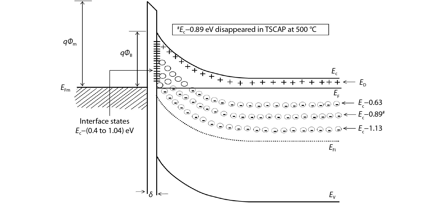
Two deep level bulk traps such as P1 (EC – 0.63 eV, Z1/2) and P2 (EC – 1.13 eV, EH5) are detected in the non-irradiated SBDs with concentrations in the 1013 cm−3 range[
![]()
Figure 1.The energy location of the bulk traps (
In non-irradiated SBDs, inhomogeneous[
The effective doping concentration of 4H-SiC epilayer is decreased (from 5 × 10¹⁴ to 3.8 × 1014 cm−3) after irradiation due to the compensation of the donor dopants by the irradiation produced acceptor-like deep level traps[
3.2. SBD characteristics after annealing
Fig. 2 shows the TSCAP spectrum of the gamma irradiated Ni/4H-SiC SBDs at different annealing temperatures from 400 to 600 °C. The increasing TSCAP steps (P1, P2 and G420) in Fig. 2 reveal the electron traps in the SBD[
where
where
Fig. 3 displays the forward current-voltage (IF–VF) characteristics of the gamma irradiated Ni/4H-SiC SBDs for the annealing temperatures of 400 to 800 °C. The forward current is found to decrease with the annealing temperature. The variations in the forward voltage drop (VF) at 1 mA, SBH, and ideality factor (n) of the SBDs are determined[
![]()
Figure 2.(Color online) Changes in the TSCAP spectrum for gamma irradiated Ni/4H-SiC SBDs at different annealing temperatures from 400 to 600 °C.
![]()
Figure 3.(Color online) Annealing effects (400–800 °C) on forward current–voltage (
To understand the abnormal variations in the post-annealing characteristics, the interface state density (NSS) distribution in the annealed SBDs is computed[
where
where
where
Fig. 5 depicts the distribution profile of the interface state density (NSS) as a function of EC – ESS for the annealed (400 – 700 °C) SBDs. Like non-irradiated 4H-SiC SBDs[
![]()
Figure 4.(Color online) Changes in the
The annealing (400–700 °C) induced changes in the reverse current–voltage (IR–VR) characteristics of the gamma irradiated Ni/4H-SiC SBDs are shown in Fig. 6. A substantial reduction in the reverse current is noticed at 400 °C due to the improvement in the SBH. Overall, the electrical parameters are improved upon the heat treatment at 400 °C, similar to the non-irradiated Ni/4H-SiC SBDs[
![]()
Figure 5.(Color online) The distribution of interface state density (
Fig. 7 shows the (1/C2)–V characteristics at 1 MHz of the gamma irradiated Ni/4H-SiC SBDs after the heat treatments (400–700 °C). It is noticed that 1/C2 increases (capacitance decreases) with the annealing temperature. Hence, the annealing induced decrease in the capacitance is the reason for the downward movement of the post-annealing TSCAP spectrum seen in Fig. 2. The (1/C2)–V characteristics at different signal frequencies (1 kHz to 1 MHz) for the SBDs at the annealing temperatures 400 and 500 °C are shown in Fig. 8 and in the inset. Similar to the pre-annealing case, frequency dependent (1/C2)–V characteristics are obtained at 400 °C. It should be noted that the computed[
![]()
Figure 6.(Color online) Annealing (400–700 °C) induced changes in the reverse current–voltage (
The decrease in the 1/C2 viewed in Fig. 8 with the signal frequency indicates the presence of acceptor-like interface traps in the SBDs. As a result, including the contribution of acceptor-like interface traps, reduced capacitance value (increased 1/C2) is obtained at low signal frequencies. Consequently, the measured capacitance increases with the signal frequency, as noted from Fig. 8. To minimize the interface state’s charge contribution, the annealing induced changes in the effective doping concentration are evaluated from the (1/C2) –V characteristics at the high signal frequency of 1 MHz. It is identified from Fig. 7 that the effective doping concentration is found to decrease with the annealing temperature (see Table 1). The effective doping concentration is reduced to 3.16 × 1014 cm−3 at 400 °C. Since the concentration of the deep level defects is not increased after the annealing, the donor concentration in the 4H-SiC epilayer must not be affected by them. In fact, the effective doping concentration is underestimated after annealing due to the contribution of the acceptor-like interface states. Strong frequency dependent (1/C2)–V characteristics perceived at 500 °C (see the inset of Fig. 8) also reveal the creation of the acceptor-like interface traps after annealing. Accordingly, the effective doping concentration at 700 °C is undervalued (~1 × 1014cm−3) by about four times its pre-annealing value.
![]()
Figure 7.(Color online) (1/
![]()
Figure 8.(Color online) (1/
Fig. 9 shows the C–V characteristics of the gamma irradiated Ni/4H-SiC SBDs for the heat treatments ≥ 800 °C (up to 1100 °C). A minor variation in the capacitance is noted with the bias voltage. However, these capacitance values are in the order of the diode geometrical capacitance[
![]()
Figure 9.Typical
Fig. 10 shows the typical I–V characteristics (−20 to 20 V) of the gamma irradiated Ni/4H-SiC SBDs at the annealing temperature of 950 °C. Very low forward current (0.54 nA at 5 V and 1.74 µA at 10 V) is obtained at 950 °C. Furthermore, undesirable electrical parameters (VF at 1 mA > ~4 V, SBH < 1 eV, and n > 8) are identified for the SBDs annealed ≥ 800 °C (see Table 1). So, the I–V and C–V characteristics state that the rectifying properties of the SBDs have vanished from the annealing temperature of 800 °C. It is reported[
![]()
Figure 10.Typical
4. Conclusion
Thermal annealing induced changes in the gamma irradiated Ni/4H-SiC SBD properties are investigated over a wide range of temperatures 400–1100 °C. The concentration of the trap at EC–0.89 eV is reduced (< 1013cm−3) below the detection limit of the TSCAP technique at the annealing temperature of 500 °C; the reduced trap density for G420 upon annealing at 500 °C may be beneficial in terms of minimizing the charge trapping effects in the real epitaxial 4H-SiC SBD detectors. On the other hand, no considerable changes in the trap density for EC–0.63 eV and EC–1.13 eV are identified up to 600 °C. Like non-irradiated Ni/4H-SiC SBDs (with Ti based Ohmic contact), the electrical characteristics are improved at 400 °C with the disappearance of dual SBH nature and the reduction in the interface trap density. Hence, the optimum annealing temperature for these kinds of Ni/4H-SiC SBD structures is ~400 °C. Nevertheless, from 500 °C, the electrical characteristics are found to degrade with the annealing temperature due to the increase in the interface state density. Reasonable electrical properties are noted up to 600 °C and finally, the SBD rectification has disappeared from 800 °C.
Acknowledgment
The authors would like to thank CSIR-CEERI for providing facilities for SBD fabrication. We also would like to thank Dr. Abhijit Saha, UGC-DAE CSR, Kolkata, for the gamma irradiation of SBDs.
References
[1]
[2] X Xin, F Yan, T W Koeth et al. Demonstration of 4H-SiC UV single photon counting avalanche photodiode. Electron Lett, 41, 212(2005).
[3] J E Lees, D J Bassford, E J Bunce et al. Silicon carbide X-ray detectors for planetary exploration. Nucl Instr Meth Phys Res A, 604, 174(2009).
[4]
[5] P V Raja, N V L N Murty. Thermally stimulated capacitance in gamma irradiated epitaxial 4H-SiC schottky barrier diodes. J Appl Phys, 123, 161536(2018).
[6] A Castaldini, A Cavallini, L Rigutti et al. Low temperature annealing of electron irradiation induced defects in 4H-SiC. Appl Phys Lett, 85, 3780(2004).
[7] N Iwamoto, B C Johnson, T Ohshima et al. Annealing effects on charge collection efficiency of an electron-irradiated 4H-SiC particle detector. 10th international workshop on radiation effects on semiconductor devices for space applications (RASEDA-10), 42(2013).
[8]
[9] F Roccaforte, F La Via, A Baeri et al. Structural and electrical properties of Ni/Ti schottky contacts on silicon carbide upon thermal annealing. J Appl Phys, 96, 4313(2004).
[10] A M Strel’chuk, A V Davydov, J Tringe et al. Characteristics of He+-irradiated Ni schottky diodes based on 4H-SiC epilayer grown by sublimation. Phys Status Solidi C, 6, 2876(2009).
[11] S K Gupta, A Azam, J Akhtar. Improved electrical parameters of vacuum annealed Ni/4H-SiC (0001) schottky barrier diode. Physica B, 406, 3030(2011).
[12] S K Gupta, N Pradhan, C Shekhar et al. Design, fabrication, and characterization of Ni/4H-SiC (0001) schottky diodes array equipped with field plate and floating guard ring edge termination structures. IEEE Trans Semicond Manuf, 25, 664(2012).
[13] V Kumar, N Kaminski, A S Maan et al. Capacitance roll-off and frequency-dispersion capacitance-conductance phenomena in field plate and guard ring edge-terminated Ni/SiO2/4H-nSiC schottky barrier diodes. Phys Status Solidi A, 213, 193(2016).
[14] V Kumar, A S Maan, J Akhtar. Tailoring surface and electrical properties of Ni/4H-nSiC schottky barrier diodes via selective swift heavy ion irradiation. Phys Status Solidi A, 215, 1700555(2018).
[15] L Huang, B Liu, Q Zhu et al. Low resistance Ti Ohmic contacts to 4H-SiC by reducing barrier heights without high temperature annealing. J Appl Phys, 100, 263503(2012).
[16] A Kcstle, S P Wilks, P R Dunstan et al. Improved Ni/SiC Schottky diode formation. Electron Lett, 36, 267(2000).
[17] M Sochacki, J Szmidt, M Bakowski et al. Influence of annealing on reverse current of 4H-SiC schottky diodes. Diamond Relat Mater, 11, 1263(2002).
[18] R Pérez, N Mestres, J Montserrat et al. Barrier inhomogeneities and electrical characteristics of Ni/Ti bilayer schottky contacts on 4H-SiC after high temperature treatments. Phys Status Solidi A, 202, 692(2005).
[19] R Pe′rez, N Mestres, D Tournier et al. Ni/Ti ohmic and Schottky contacts on 4H-SiC formed with a single thermal treatment. Diamond Relat Mater, 14, 1146(2005).
[20] L Calcagno, A Ruggiero, F Roccaforte et al. Effects of annealing temperature on the degree of inhomogeneity of nickel-silicide/SiC schottky barrier. J Appl Phys, 98, 023713(2005).
[21] T N Oder, P Martin, A V Adedeji et al. Improved schottky contacts on n-type 4H-SiC using ZrB2 deposited at high temperatures. J Electron Mater, 36, 805(2007).
[22] T N Oder, T L Sung, M Barlow et al. Improved Ni schottky contacts on n-type 4H-SiC using thermal processing. J Electron Mater, 38, 772(2009).
[23] C K Ramesha, V R Reddy. Influence of annealing temperature on the electrical and structural properties of palladium schottky contacts on n-type 4H-SiC. Superlattices Microstruct, 76, 55(2014).
[24] L C Han, H J Sun, K A Liu et al. Annealing temperature influence on the degree of inhomogeneity of the schottky barrier in Ti/4H-SiC contacts. Chin Phys B, 23, 127302(2014).
[25] G Pristavu, G Brezeanu, M Badila et al. A model to non-uniform Ni schottky contact on SiC annealed at elevated temperatures. Appl Phys Lett, 106, 261605(2015).
[26] S Kyoung, E Jung, M Y Sung. Post-annealing processes to improve inhomogeneity of schottky barrier height in Ti/Al 4H-SiC schottky barrier diode. Microelectron Eng, 154, 69(2016).
[27] S B Yun, J H Kim, Y H Kang et al. Optimized annealing temperature of Ti/4H-SiC schottky barrier diode. J Nanosci Nanotechnol, 17, 3406(2017).
[28] L Storasta, H Tsuchida, T Miyazawa et al. Enhanced annealing of the Z1/2 defect in 4H-SiC epilayers. J Appl Phys, 103, 013705(2008).
[29] M A Mannan, K V Nguyen, R O Pak et al. Deep levels in n-type 4H-silicon carbide epitaxial layers investigated by deep-level transient spectroscopy and isochronal annealing studies. IEEE Trans Nucl Sci, 63, 1083(2016).
[30] P V Raja, J Akhtar, C V S Rao et al. Spectroscopic performance studies of 4H-SiC detectors for fusion alpha-particle diagnostics. Nucl Instrum Methods Phys Res A, 869, 118(2017).
[31] P V Raja, N V L N Murty. Thermal annealing studies in epitaxial 4H-SiC schottky barrier diodes over wide temperature range. Microelectron Reliab, 87, 213(2018).
[32] M Sochacki, A Kolendo, J Szmidt et al. Properties of Pt/4H-SiC schottky diodes with interfacial layer at elevated temperatures. Solid State Electron, 49, 585(2005).
[33] M Bhatnagar, B J Baliga, H R Kirk et al. Effect of surface inhomogeneities on the electrical characteristics of SiC Schottky contacts. IEEE Trans Electron Devices, 43, 150(1996).
[34] D Defives, O Noblanc, C Dua et al. Barrier inhomogeneities and electrical characteristics of Ti/4H-SiC Schottky rectifiers. IEEE Trans Electron Devices, 46, 449(1999).
[35] Q Zhang, T S Sudarshan. The influence of high-temperature annealing on SiC Schottky diode characteristics. J Electron Mater, 30, 1466(2001).
[36] D V Lang. Space-charge spectroscopy in semiconductors. In: Thermally stimulated relaxation in solids. Berlin: Springer, 93(1979).
[37] G L Miller, D V Lang, L C Kimerling. Capacitance transient spectroscopy. Ann Rev Mater Sci, 7, 377(1977).
[38]
[39] T Dalibor, G Pensl, H Matsunami et al. Deep defect centers in silicon carbide monitored with deep level transient spectroscopy. Phys Status Solidi A, 162, 199(1997).
[40]
[41] S Y Han, K H Kim, J K Kim et al. Ohmic contact formation mechanism of Ni on n-type 4H-SiC. Appl Phys Lett, 79, 1816(2001).
[42] S Y Han, J Lee. Effect of interfacial reactions on electrical properties of Ni contacts on lightly doped n-type 4H-SiC. J Electrochem Soc, 149, G189(2002).
[43] S Y Han, J Shin, B Lee et al. Microstructural interpretation of Ni ohmic contact on n-type 4H-SiC. J Vac Sci Technol B, 20, 1496(2002).
[44] S U Omar, T S Sudarshan, T A Rana et al. Interface trap-induced nonideality in as-deposited Ni/4H-SiC schottky barrier diode. IEEE Trans Electron Devices, 62, 615(2015).
[45] J H Zhao, K Sheng, R C Lebron-Velilla. Silicon carbide Schottky barrier diode. Int J High Speed Electron, 15, 821(2005).
[46] D H Kim, J H Lee, J H Moon et al. Improvement of the reverse characteristics of Ti/4H-SiC Schottky barrier diodes by thermal treatments. Solid State Phenom, 124-126, 105(2007).


Set citation alerts for the article
Please enter your email address

© Copyright 2018-2021 | Chinese Laser Press. All Rights Reserved 沪ICP备15018463号-20