• Photonics Research
  • Vol. 10, Issue 10, 2267 (2022)
Yang Xu1, Yulu Qin1、2, Peng Lang1, Boyu Ji1, Xiaowei Song1, and Jingquan Lin1、*
Author Affiliations
  • 1School of Science, Changchun University of Science and Technology, Changchun 130022, China
  • 2State Key Laboratory for Mesoscopic Physics and Collaborative Innovation Center of Quantum Matter, Department of Physics, Peking University, Beijing 100871, China
  • show less
    DOI: 10.1364/PRJ.460638 Cite this Article Set citation alerts
    Yang Xu, Yulu Qin, Peng Lang, Boyu Ji, Xiaowei Song, Jingquan Lin. Flexible manipulation of plasmon dephasing time via the adjustable Fano asymmetric dimer[J]. Photonics Research, 2022, 10(10): 2267 Copy Citation Text show less
    Experimental setup and the characterization of Au nanostructure. (a) Structure of gold asymmetric nanorod dimer. L, W, H, and D are the length, width, height, and gap size, respectively. L1 and L2 are the lengths of upper and lower nanorods, respectively. W = 80 nm, H = 60 nm, and D = 50 nm remain unchanged. (b) SEM images of the asymmetric nanorod dimer; the scale bar in the inset is 200 nm.
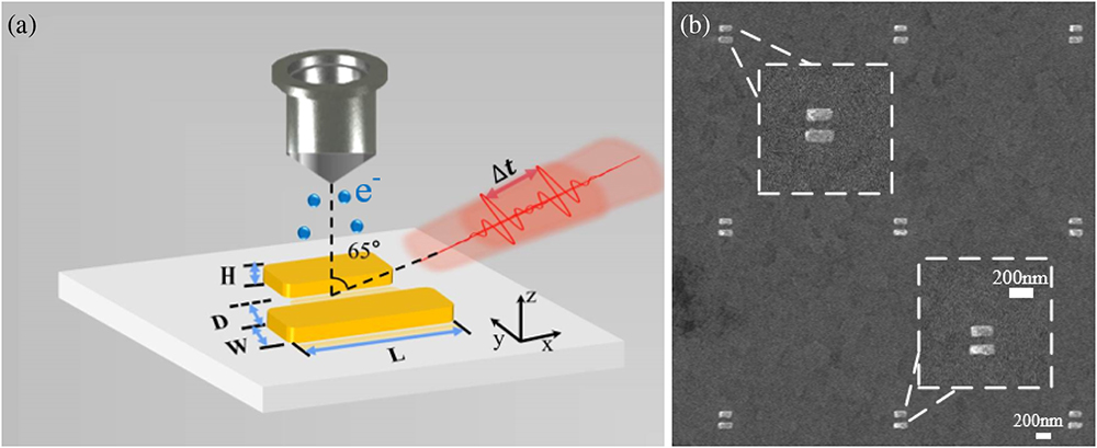
    Fig. 1. Experimental setup and the characterization of Au nanostructure. (a) Structure of gold asymmetric nanorod dimer. L, W, H, and D are the length, width, height, and gap size, respectively. L1 and L2 are the lengths of upper and lower nanorods, respectively. W=80  nm, H=60  nm, and D=50  nm remain unchanged. (b) SEM images of the asymmetric nanorod dimer; the scale bar in the inset is 200 nm.
    Near-field and far-field properties and ultrafast dynamics of the three structures. (a) Normalized experimental near-field spectra of the isolated nanorod (L = 195 nm), symmetric nanorod dimers (L1 = L2 = 195 nm), and asymmetric nanorod dimers (L1 = 165 nm, L2 = 195 nm) with corresponding simulated far-field scattering spectra. The near-field (∫|E(t)|6dt) spectrum of the asymmetric nanorod dimer is simulated by FDTD as shown in the red dotted line. The left insets are corresponding experiment PEEM images and the simulated PEEM images obtained by calculation (∫|E(t)|6dt) in the plane of incidence. The red arrow indicates the polarization of the excitation light along the x-axis as p-polarization. The right insets show the simulated charge distribution of the corresponding structures. The bottom is the double-logarithmic plot of the integrated photoemission signal versus the laser power yielding a slope of 3.15 in a linear fitting for the asymmetric nanorod dimer. (b) Corresponding PE intensity as a function of delay time between pump and probe pulses with fitted dephasing times.
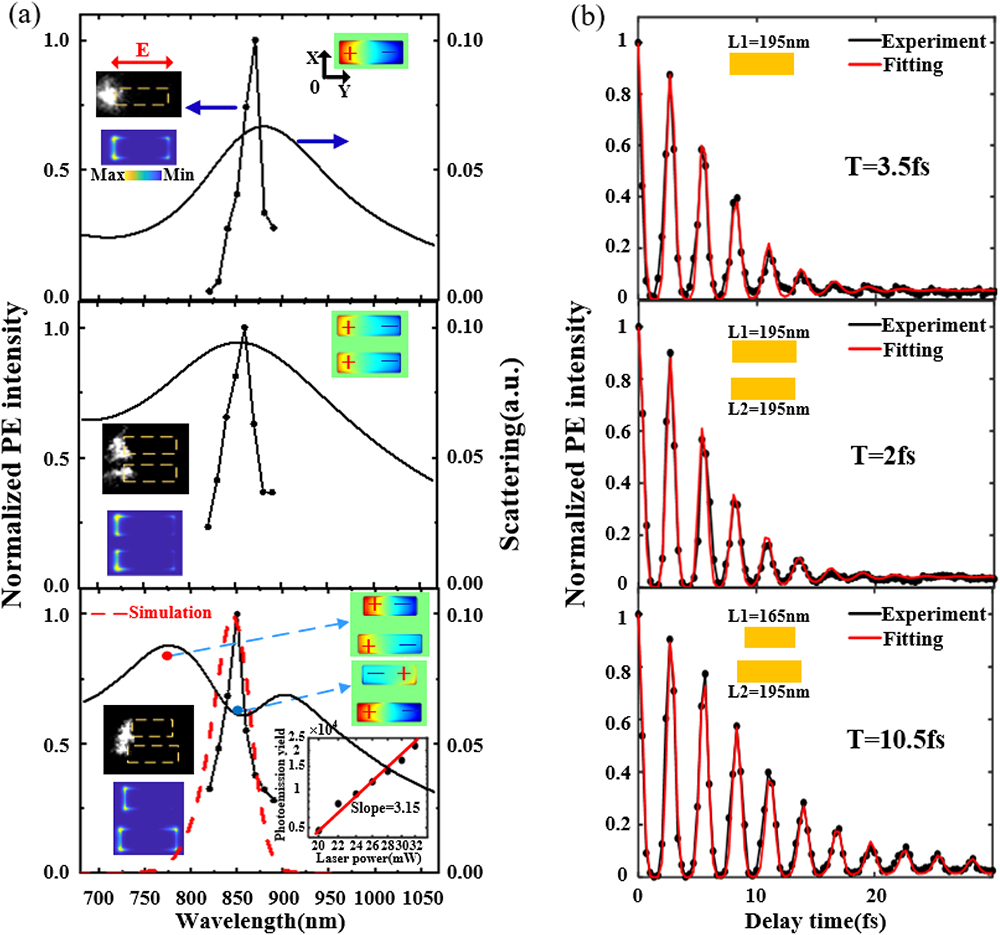
    Fig. 2. Near-field and far-field properties and ultrafast dynamics of the three structures. (a) Normalized experimental near-field spectra of the isolated nanorod (L=195  nm), symmetric nanorod dimers (L1=L2=195  nm), and asymmetric nanorod dimers (L1=165  nm, L2=195  nm) with corresponding simulated far-field scattering spectra. The near-field (|E(t)|6dt) spectrum of the asymmetric nanorod dimer is simulated by FDTD as shown in the red dotted line. The left insets are corresponding experiment PEEM images and the simulated PEEM images obtained by calculation (|E(t)|6dt) in the plane of incidence. The red arrow indicates the polarization of the excitation light along the x-axis as p-polarization. The right insets show the simulated charge distribution of the corresponding structures. The bottom is the double-logarithmic plot of the integrated photoemission signal versus the laser power yielding a slope of 3.15 in a linear fitting for the asymmetric nanorod dimer. (b) Corresponding PE intensity as a function of delay time between pump and probe pulses with fitted dephasing times.
    Near-field properties and ultrafast dynamics of asymmetric nanorod dimers with the increase of length L1 (fixed L2) from PEEM measurements. (a) Comparison of normalized near-field spectra for asymmetric nanorod dimers [L1 = 120 nm, L2 = 165 nm (blue curve); L1 = 135 nm, L2 = 165 nm (black curve); L1 = 150 nm, L2 = 165 nm (red curve)] with fixed L2 and increased L1. (b)–(d) Corresponding PE intensity as a function of delay time between pump and probe pulses with fitted dephasing times. The inset shows the scattering spectra of the corresponding three structures.
    Fig. 3. Near-field properties and ultrafast dynamics of asymmetric nanorod dimers with the increase of length L1 (fixed L2) from PEEM measurements. (a) Comparison of normalized near-field spectra for asymmetric nanorod dimers [L1=120  nm, L2=165  nm (blue curve); L1=135  nm, L2=165  nm (black curve); L1=150  nm, L2=165  nm (red curve)] with fixed L2 and increased L1. (b)–(d) Corresponding PE intensity as a function of delay time between pump and probe pulses with fitted dephasing times. The inset shows the scattering spectra of the corresponding three structures.
    Near-field properties and ultrafast dynamics of asymmetric nanorod dimers with the increase of length L2 (fixed L1) from PEEM measurements. (a) Comparison of normalized near-field spectra for asymmetric nanorod dimers [L1 = 150 nm, L2 = 165 nm (red curve); L1 = 150 nm, L2 = 180 nm (yellow curve); L1 = 150 nm, L2 = 195 nm (purple curve)] with fixed L1 and increased L2. (b), (c) Corresponding PE intensity as a function of delay time between pump and probe pulses with fitted dephasing times. The inset shows the scattering spectra of the corresponding three structures. (d) The variation trend of resonance wavelength and dephasing time under the separate variation lengths L1 and L2. The black and red lines represent changes in resonance wavelength and dephasing time, respectively, and the solid and the dashed lines are the result of simulation and experiment, respectively. The top inset shows that the plasmon electric field intensity of the (L1 = 150 nm, L2 = 180 nm) asymmetric nanorod dimer decays with time after light excitation is stopped. The monitor position is shown as a red circle in the simulated PEEM images at resonance wavelength in the bottom inset. The simulated near-field spectrum is also shown in the bottom inset.
    Fig. 4. Near-field properties and ultrafast dynamics of asymmetric nanorod dimers with the increase of length L2 (fixed L1) from PEEM measurements. (a) Comparison of normalized near-field spectra for asymmetric nanorod dimers [L1=150  nm, L2=165  nm (red curve); L1=150  nm, L2=180  nm (yellow curve); L1=150  nm, L2=195  nm (purple curve)] with fixed L1 and increased L2. (b), (c) Corresponding PE intensity as a function of delay time between pump and probe pulses with fitted dephasing times. The inset shows the scattering spectra of the corresponding three structures. (d) The variation trend of resonance wavelength and dephasing time under the separate variation lengths L1 and L2. The black and red lines represent changes in resonance wavelength and dephasing time, respectively, and the solid and the dashed lines are the result of simulation and experiment, respectively. The top inset shows that the plasmon electric field intensity of the (L1=150  nm, L2=180  nm) asymmetric nanorod dimer decays with time after light excitation is stopped. The monitor position is shown as a red circle in the simulated PEEM images at resonance wavelength in the bottom inset. The simulated near-field spectrum is also shown in the bottom inset.
    Comparison of plasmon resonance wavelength and dephasing time for different asymmetric nanorod dimers from simulation and calculation. (a) The variation trend of resonance wavelength and dephasing time under the separate variation lengths L1 and L2 in different structures (L1 = 135 nm, L2 = 165 nm; L1 = 150 nm, L2 = 165 nm; L1 = 160 nm, L2 = 165 nm; L1 = 135 nm, L2 = 180 nm; L1 = 135 nm, L2 = 195 nm). (b) The variation trend of resonance wavelength and dephasing time under the variation of both lengths L1 and L2 (L1 = 120 nm, L2 = 165 nm; L1 = 135 nm, L2 = 180 nm; L1 = 150 nm, L2 = 195 nm). The inset shows the scattering spectra of the corresponding three structures. The black and red lines represent changes in resonance wavelength and dephasing time, respectively.
    Fig. 5. Comparison of plasmon resonance wavelength and dephasing time for different asymmetric nanorod dimers from simulation and calculation. (a) The variation trend of resonance wavelength and dephasing time under the separate variation lengths L1 and L2 in different structures (L1=135  nm, L2=165  nm; L1=150  nm, L2=165  nm; L1=160  nm, L2=165  nm; L1=135  nm, L2=180  nm; L1=135  nm, L2=195  nm). (b) The variation trend of resonance wavelength and dephasing time under the variation of both lengths L1 and L2 (L1=120  nm, L2=165  nm; L1=135  nm, L2=180  nm; L1=150  nm, L2=195  nm). The inset shows the scattering spectra of the corresponding three structures. The black and red lines represent changes in resonance wavelength and dephasing time, respectively.
    Simulated optical response of the asymmetric nanorod dimer (L1 = 150 nm, L2 = 180 nm) with the decrease in the gap size D. (a) Normalized near-field spectra of the asymmetric nanorod dimers with D = 50 nm (blue curve), D = 40 nm (purple curve), and D = 30 nm (yellow curve). The lengths of L1 and L2 are fixed at L1 = 150 nm and L2 = 180 nm. (b), (c) The normalized electric field decays with time after light excitation suddenly stopped for asymmetric nanorod dimers with D = 40 nm and D = 30 nm, respectively. The inset in (b) shows a custom suddenly cutting CW source signal with a carrier wavelength of 835 nm, corresponding to the plasmon resonance wavelength of the asymmetric nanorod dimer of D = 40 nm. It should be noted that the carrier wavelength of the light source is selected according to the plasmon resonance wavelength of the structures. (d) The corresponding scattering spectra of the asymmetric nanorod dimers with three gap sizes.
    Fig. 6. Simulated optical response of the asymmetric nanorod dimer (L1 = 150 nm, L2 = 180 nm) with the decrease in the gap size D. (a) Normalized near-field spectra of the asymmetric nanorod dimers with D = 50 nm (blue curve), D = 40 nm (purple curve), and D = 30 nm (yellow curve). The lengths of L1 and L2 are fixed at L1 = 150 nm and L2 = 180 nm. (b), (c) The normalized electric field decays with time after light excitation suddenly stopped for asymmetric nanorod dimers with D = 40 nm and D = 30 nm, respectively. The inset in (b) shows a custom suddenly cutting CW source signal with a carrier wavelength of 835 nm, corresponding to the plasmon resonance wavelength of the asymmetric nanorod dimer of D = 40 nm. It should be noted that the carrier wavelength of the light source is selected according to the plasmon resonance wavelength of the structures. (d) The corresponding scattering spectra of the asymmetric nanorod dimers with three gap sizes.
    Yang Xu, Yulu Qin, Peng Lang, Boyu Ji, Xiaowei Song, Jingquan Lin. Flexible manipulation of plasmon dephasing time via the adjustable Fano asymmetric dimer[J]. Photonics Research, 2022, 10(10): 2267
    Download Citation