1School of Science, Changchun University of Science and Technology, Changchun 130022, China
2State Key Laboratory for Mesoscopic Physics and Collaborative Innovation Center of Quantum Matter, Department of Physics, Peking University, Beijing 100871, China
Yang Xu, Yulu Qin, Peng Lang, Boyu Ji, Xiaowei Song, Jingquan Lin, "Flexible manipulation of plasmon dephasing time via the adjustable Fano asymmetric dimer," Photonics Res. 10, 2267 (2022)
Copy Citation Text
It is highly desirable to flexibly and actively manipulate the dephasing time of a plasmon in many potential applications; however, this remains a challenge. In this work, by using femtosecond time-resolved photoemission electron microscopy, we experimentally demonstrated that the Fano resonance mode in the asymmetric nanorod dimer can greatly extend the dephasing time of a femtosecond plasmon, whereas the non-Fano resonance results in a smaller dephasing time due to the large radiative damping, and flexible manipulation of the dephasing time can be realized by adjusting one of the nanorods in the Fano asymmetric dimer. Interestingly, it was found that plasmon resonance wavelengths both appeared red-shifted as the length of the upper or lower nanorods increased individually, but the dephasing time varied. Furthermore, it also indicated that the dephasing time can be prolonged with a smaller ascending rate by increasing the length of both the nanorods simultaneously while keeping the dimer asymmetry. Meanwhile, the roles of radiative and nonradiative damping in dephasing time are unveiled in the process of nanorod length variation. These results are well supported by numerical simulations and calculations.
1. INTRODUCTION
As the core parameter of localized surface plasmon resonances (LSPRs) [1,2], plasmon dephasing time [3] plays a pivotal role in a wide range of fields, such as photodevice [4,5], chemosensing [6], and biomedicine [7]. In particular, long plasmon dephasing time is required to greatly promote surface-enhanced Raman scattering (SERS) [8] and emerging sensor sensitivity [9–11]. Meanwhile, for femtosecond-scale plasmon optical switching devices and ultrafast electron vortex beams [12,13], the requirement of a relatively short dephasing time is expected. To achieve this, flexible and on-demand manipulation of the dephasing time is highly desirable.
Recently, researchers have studied the plasmon dephasing time, including increasing the length of the single rod [14] and stacked structure [15] to reduce nonradiative damping, decreasing the disk/rod dimer gap [16] to enhance radiative damping, turning polarization to make plasmon modes of block [17] and bowtie [18] change to alter radiative damping, and adjusting the array period to enhance the energy exchange between the LSP and surface plasmon polariton [19,20]. Despite the above-mentioned progress, in those schemes, the dephasing time can only be changed monotonously (only either by increasing or decreasing) due to the limitation of the manipulation parameter, leading to the lack of flexible control of the dephasing time. In addition, it should be noted that, generally, the change of the dephasing time is accompanied by the shift of the plasmon resonance wavelength, both of which are closely related to ultrafast electron pulses [21], plasmon nanolasers [22,23], and single-molecule detection [24]. Therefore, the flexible control of the dephasing time should simultaneously consider the plasmon resonance wavelength, that is, the goal is to achieve that, as the resonance wavelength shifts in a certain direction, the dephasing time can have different variation trends, enabling both increase and decrease, which is the basis for the construction of low-threshold, pulse-width/wavelength adjustable nano-lasers and ultra-fast nano-electronic point sources, and also it greatly benefits the optimization of solar cell energy harvesting [25–27] and the on-demand control of the sensitivity of sensing and single-molecule detection. However, the current research on the dephasing time often neglects the coordinated change of the related resonance wavelength, and the dephasing time cannot be manipulated flexibly and on-demand, which hinders the design and development of the above-mentioned plasmonic optoelectronic devices.
This paper investigated the manipulation of plasmon dephasing time and resonance wavelength of Fano gold asymmetric nanorod dimers using time-resolved photoemission electron microscopy (TR-PEEM) [28–30]. We compared the dephasing times of Fano and non-Fano plasmon modes in asymmetric and symmetric nanorod dimers respectively. The results show that the Fano resonance dark mode greatly prolongs the dephasing time, whereas the non-Fano resonance results in a smaller dephasing time due to the large radiative damping. More importantly, we find that the flexible manipulation of the dephasing time can be realized by adjusting the length of the upper or lower nanorod in the Fano asymmetric dimer.
Sign up for Photonics Research TOC. Get the latest issue of Photonics Research delivered right to you!Sign up now
The results indicate that plasmon resonance wavelengths both appear red-shifted as the length of the upper or lower nanorods increases individually, but a different variation trend of the dephasing time is found. In particular, it is realized that the same dephasing time can be obtained at different resonance wavelengths and even different dephasing times can be achieved under the same wavelength by optimizing the size of the nanorod dimer. Moreover, it was found that the dephasing time of the Fano asymmetric dimer can be prolonged with a small ascending rate by increasing the length of both nanorods simultaneously, while keeping the length asymmetry unchanged. Meantime, we qualitatively analyzed the influence of radiative and nonradiative damping on the dephasing time when adjusting different parameters. The experimental results are supported by the radiative damping calculations and finite-difference time-domain (FDTD) simulations.
2. RESULTS AND DISCUSSION
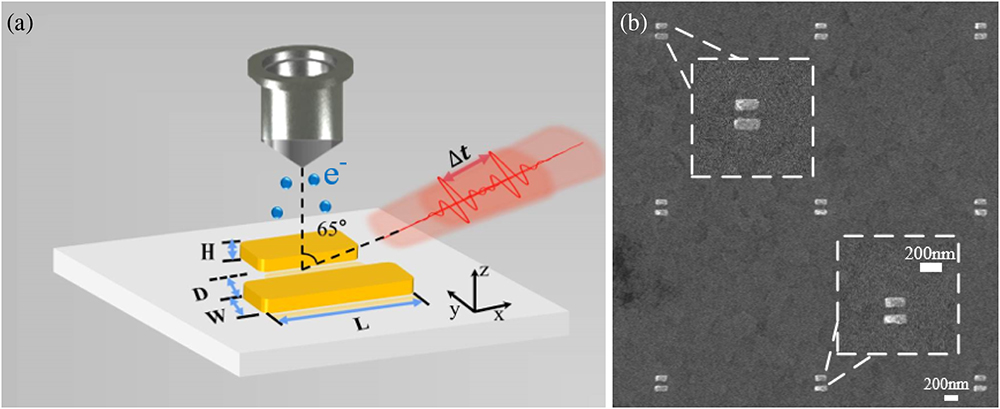
A series of Au nanorod dimer arrays of different sizes were fabricated using electron-beam lithography followed by metal sputtering and a lift-off process. The experimental setup (see Section 4 for details) and the characterization of Au asymmetric nanorod dimer are schematically presented in Fig. 1(a). The p-polarization pulses illuminate the sample along the -axis direction at an incidence angle of 65° from the right side. Dimers are arranged in a two-dimensional square array with a 2 μm pitch size on the 150-nm-thick indium tin oxide (ITO)-layer-covered glass substrate. , , , and represent the length, width, height, and gap size of the dimer, respectively ( and are lengths of upper and lower nanorods, respectively). Throughout the paper, , , and remain unchanged. A typical scanning electron microscopy (SEM) image of the asymmetric nanorod dimers is presented in Fig. 1(b). It should be mentioned that the field of view (FOV) used in the subsequent TR-PEEM measurements of asymmetric nanorod dimers is 6 μm. The TR-PEEM measurements for the averaged overall structures within the FOV and several individual structural units were compared. The results indicate that the measured photoemission (PE) signals versus delay time (PE curve) of individual structural units overlap well with the averaged PE curve of the overall structures (details not shown here), which indicates a good homogeneity of the plasmonic units within the FOV. This demonstrates that the quantitative analysis of the dephasing time based on the averaged TR-PEEM measurements is reliable.
Figure 1.Experimental setup and the characterization of Au nanostructure. (a) Structure of gold asymmetric nanorod dimer. , , , and are the length, width, height, and gap size, respectively. and are the lengths of upper and lower nanorods, respectively. , , and remain unchanged. (b) SEM images of the asymmetric nanorod dimer; the scale bar in the inset is 200 nm.
Typical PEEM images in the small field of view of an isolated nanorod (), symmetric (), and asymmetric (, , ) nanorod dimers in an array that are irradiated by femtosecond laser pulses are presented in the left inset of Fig. 2(a). The results indicate that the intensity and position of photoemission are varied in the three structures, which correspond to different plasmon modes of the three structures. It should be mentioned that the photoelectron emission of the asymmetric nanorod dimer of and is about a three-photon photoemission process by fitting the photoemission yield as a function of laser power [the bottom inset of Fig. 2(a)]. The calculated nonlinear order of other structures with different sizes used in our experiments ranges from 2.8 to 3.2, which may result from different plasmon resonance wavelengths (not shown here).
Figure 2.Near-field and far-field properties and ultrafast dynamics of the three structures. (a) Normalized experimental near-field spectra of the isolated nanorod (), symmetric nanorod dimers (), and asymmetric nanorod dimers (, ) with corresponding simulated far-field scattering spectra. The near-field () spectrum of the asymmetric nanorod dimer is simulated by FDTD as shown in the red dotted line. The left insets are corresponding experiment PEEM images and the simulated PEEM images obtained by calculation () in the plane of incidence. The red arrow indicates the polarization of the excitation light along the -axis as p-polarization. The right insets show the simulated charge distribution of the corresponding structures. The bottom is the double-logarithmic plot of the integrated photoemission signal versus the laser power yielding a slope of 3.15 in a linear fitting for the asymmetric nanorod dimer. (b) Corresponding PE intensity as a function of delay time between pump and probe pulses with fitted dephasing times.
Figure 2(a) also exhibits the measured wavelength-dependent photoemission intensity spectra (referred to as near-field spectra) of the aforementioned isolated nanorod, symmetric and asymmetric nanorod dimers, as indicated by lines with solid circular data points. The near-field spectra show that the resonance peaks for the three structures occur at approximately 870, 860, and 850 nm, respectively. Furthermore, far-field scattering spectra, photoemission distribution, and charge distribution of the plasmon modes of the three structures were studied using the FDTD simulation. It is noted that the simulated PEEM images under resonance wavelengths are consistent with the measured one [the left insets of Fig. 2(a)]. In addition, for both isolated nanorod and symmetric nanorod dimers, the peaks of the simulated far-field scattering spectra as displayed by solid lines are almost identical to those of the respective near-field spectra. Moreover, the calculated charge distribution diagrams [the right insets of Figs. 2(a) and 2(b)] demonstrate that the plasmon modes of isolated nanorod and symmetric nanorod dimer are bright modes with a typical wide scattering spectrum induced by the radiative damping of the dipole. The charge of the two nanorods in symmetric nanorods dimer is in-phase distribution, resulting in an even superradiant plasmon mode with much higher radiative damping.
However, for the asymmetric nanorod dimer, as shown in the low panel of Fig. 2(a), the simulated scattering spectrum shows a Fano line shape with two scattering resonance peaks, while the experimental near-field spectrum peak approximately corresponds to the scattering spectrum dip position. In addition, the near-field () spectrum of the asymmetric nanorod dimer is simulated by FDTD, as shown in the red dotted line in Fig. 2(a), which is generally consistent with the experimental near-field spectrum, with only one near-field resonance peak in the wavelength range of 680–950 nm. Notably, the spectrum dip indicates that the Fano resonance is induced by the near-field coupling between the upper and lower nanorods due to the introduction of structural symmetry breaking [31,32]. In our asymmetric plasmonic structure, the nanorod dimer can resonantly induce symmetric or asymmetric electron oscillations modes depending on the driving frequency with the incident electric field polarized along the major axis of the nanorod [33]. When the two nanorods are the same length, it is easy to directly excite and radiate the symmetric plasmon bright mode and the whole structure shows dipole oscillations. In contrast, the asymmetric plasmon dark mode can be indirectly induced through coupling with the bright resonator with a length asymmetry. To better understand the physical origins of Fano resonance in an asymmetric nanorod dimer, the charge distributions at 760 nm (broad resonance peak) and 850 nm (Fano dip corresponds to the near-field spectrum peak) are shown in the right insets of the bottom panel of Fig. 2(a). It is clear that the in-phase charge distribution (bright plasmon mode) appears in two parallel nanorods at the wavelength of 760 nm, while the out-of-phase charge distribution (dark plasmon mode) appears at the wavelength of 850 nm, which can only be indirectly excited by coupling with the radiative bright plasmon mode. It demonstrates that the Fano resonance is caused by destructive interference of a bright mode and a dark mode in the system. It is noted that only dark mode is observed in the near-field spectrum in the bottom panel of Fig. 2(a). This is because the Fano resonance formed by the coupling of bright mode and dark mode in the asymmetric nanorod dimers will cause the bright mode to transfer its energy around the frequency corresponding to the dip of the scattering spectrum to the dark mode excitation [31], and the effect of the bright mode is canceled by the destructive interference in the coupling. This results in an asymmetric Lorentzian line-type scattering spectrum and an extremely higher near-field intensity for dark mode around the frequency of Fano resonance dip than the field at other frequencies for our case. Similar results were observed in the previous works [15,34]. Consequently, only a resonance peak corresponding to the dark mode can be found in the near-field spectrum in the bottom panel of Fig. 2(a). We should mention that this process is different from the one of plasmon-induced transparency (PIT) supported by the dolmen structure [35], even though they present a configuration similar in geometry and profile in the scattering spectrum [36]. It should be mentioned that all asymmetric nanorod dimers used in the following work have been verified to support Fano resonance.
In addition, it needs to be mentioned that the measured near-field spectra in Fig. 2(a) are in fact wavelength-dependent photoemission intensity spectra, which are derived from the relationship of (), where is the near-field amplitude. In our case, the photoemission is approximately a three-order nonlinear process, thus resulting in a reduced bandwidth difference of the photoemission intensity spectra among the three cases in Fig. 2(a) compared with the usual near- or far-field spectra. Actually, bandwidths of the wavelength-dependent photoemission intensity spectra of the bottom, upper, and middle panels in Fig. 2(a) increase in sequence, which generally supports the decreasing trend of the dephasing time of the three plasmonic modes. It should be mentioned that the near-field spectra measured in our experiment are slightly narrower than those they should be, which may be caused by the experimental measurement error due to power fluctuations and beam drift when varying the laser carrier wavelength. The measured wavelength-dependent photoemission intensity spectra in Fig. 2(a) are mainly used to confirm the resonance wavelengths of the structure, and then to set the resonance wavelength parameters in the harmonic oscillator model in this work rather than to quantitatively evaluate the dephasing time. The harmonic oscillator model is used to fit the experimental PE curve to obtain the dephasing time in this work, which has been verified as an excellent method to accurately measure the dephasing time [15,17,20].
TR-PEEM combined with an interferometric pump-probe technique was used to measure the dephasing time. Figure 2(b) shows the TR-PEEM intensity as a function of the delay time between two pulses measured for corresponding isolated nanorod, symmetric, and asymmetric nanorod dimers. The dephasing time was fitted by applying a damped harmonic oscillator analytical model [17,37] to the experimental time-resolved PE signals. As follows, in the harmonic oscillator model, the plasmon field is written as
Here, is the driving field. In the case of interferometric pump-probe measurements, includes both the pump and probe optical fields and can be expressed as . denotes a delay between the pump and probe pulses. represents the plasmon resonance frequency. is the damping coefficient of the resonance frequency ( denotes the dephasing time). Considering the nonlinearity of the photoemission evolved in this study, the delay time ()-dependent photoemission intensity can be given as
Here, denotes the nonlinear order of the photoemission. Then, we can calculate the photoemission intensity as a function of delay time using Eq. (2) assuming a dephasing time . Compared with the experimental curves, we can obtain the best-fitted value. Based on the fact that the asymmetric nanorod dimer has only one near-field resonance peak, and the curve of photoelectron yield versus delay time does not show the obvious beating characteristics of the coupled modes, a single harmonic oscillator model is used to fit the dephasing time [15,30] in this paper.
The fitted dephasing times of the isolated nanorod and symmetric nanorod dimers are 3.5 and 2.0 fs, respectively [the upper and middle panels of Fig. 2(b)]. The results show that the dephasing time of the symmetric nanorod dimers is shorter than that of the isolated nanorod, corresponding to a wider scattering spectrum linewidth. This result suggests that stronger radiative damping is caused by the interaction of the in-phase dipole–dipole of the two rods in the symmetric dimer, resulting in a superradiant mode with the coherent addition of plasmonic dipoles. Compared to the cases of the non-Fano isolated nanorod and symmetric nanorod dimers, the result intuitively proves that the Fano resonance can greatly prolong the dephasing time to 10.5 fs [the bottom panels of Fig. 2(b)]. The out-of-phase charge distribution in two parallel nanorods reduces the overall dipole moment of asymmetric nanorod dimers, resulting in a reduced net dipole moment [38,39], and thus inhibits the strong radiative damping and leads to an enhanced dephasing time.
Figure 3 shows the effect of the upper nanorod length variation in the Fano asymmetric dimers on plasmon resonance wavelength and dephasing time. Plasmon resonance wavelengths show a red shift from 720 to 820 nm (the resonance frequency varies from 417 to 366 THz) with the increase of length from 120 to 150 nm (fixed ), as depicted in normalized near-field spectra of Fig. 3(a). With the upper nanorod lengths being 120, 135, and 150 nm (fixed ), the full width at half maximum (FWHM) () of the sixth root of the wavelength-dependent photoemission yield spectra is 33, 20, and 16 THz, respectively. The results show that the linewidths of the near-field spectra get narrow with the increase of , indicating that the overall damping of the structure decreases gradually in this process. The numerical fitting and experimental PE intensity curves with the three structures of and 150 nm are shown in Figs. 3(b)–3(d), and the best-fitted dephasing time corresponds to 6, 9, and 11 fs, respectively. Apparently, the results show that the dephasing time of the asymmetric nanorod dimer increases significantly with the increase of the length when the length remains unchanged. The PE curves for the asymmetric nanorod dimer with , and , were selected as two examples to evaluate the fitting errors of the dephasing times based on the method of fitting the harmonic oscillator model with the PE measurement curves. The results give fitting errors of (details not shown here).
Figure 3.Near-field properties and ultrafast dynamics of asymmetric nanorod dimers with the increase of length (fixed ) from PEEM measurements. (a) Comparison of normalized near-field spectra for asymmetric nanorod dimers [, (blue curve); , (black curve); , (red curve)] with fixed and increased . (b)–(d) Corresponding PE intensity as a function of delay time between pump and probe pulses with fitted dephasing times. The inset shows the scattering spectra of the corresponding three structures.
Furthermore, we also simulate the scattering spectra of the three structures [the insets of Fig. 3(d)] and then compare the linewidth of the Fano dips. It was found that as length increases (fixed ), the gradually becomes narrower, indicating that the radiative loss is more suppressed and thus it is favored for the prolongation of the dephasing time [40,41]. The linewidth (FWHM) is estimated based on the lower resonant scattering peak and the lowest scattering dip of the Fano resonance asymmetric lineshape [40]. Moreover, we estimate the overall radiative power of asymmetric nanorods dimer by simulations and calculations, which corresponds to the radiative damping. Due to the quadrupole-like charge distribution of the asymmetric nanorod dimer, the radiative field induced by a net electric dipole, quadrupole, and magnetic dipole should be taken into account to determine the main part of radiative damping of the plasmonic field [32,42–44]. The higher order of electric moment can be neglected due to their inappreciable radiative field. The electric dipole moment , electric quadrupole moment , and magnetic dipole moment are calculated, respectively [45]: where and are the electric charge density and the current density obtained by FDTD, respectively. Then the total radiative field generated by the electric dipole, the electric quadrupole, and the magnetic dipole can be obtained: where and are the vacuum conductivity and magnetic permeability, and .
Finally, the radiative power is calculated according to the formula ∯
The relative radiative power of the upper nanorod length from 120 to 150 nm is calculated as , , and , respectively, which further demonstrates that the overall radiative damping decreases with the increase of the length . In contrast, it is well known that the plasmon-dephasing results not only from radiative damping with coupling into far-field via the scattering process, but also from the nonradiative damping that can create electron–hole pairs in metal via either interband or intraband transition [46]. The increase of the length leads to the red shift of the plasmon resonance wavelength, and the red shift of the resonance wavelength causes the plasmon resonance to move away from the interband transition band () of the gold [14], thus also suppressing the nonradiative damping caused by the interband transition. In addition, we used the frequency linewidth of the Fano dip in the scattering spectrum to evaluate the dephasing time of the dark mode. The calculation results show that, with the upper nanorod length being 120, 135, and 150 nm (fixed ), the [the inset of Fig. 3(d)] are around 31, 19, and 14 THz, respectively. The calculated corresponding dephasing times are correspondingly 5.2, 8.4, and 11.4 fs, based on the relation [20], which are in good agreement with the results obtained using the damped harmonic oscillator model and the electric field exponential decay fitting [Fig. 4(d)]. Therefore, the dephasing time prolongs with wavelength red shifts in Fig. 3, which is due to the suppression of both the radiative damping and nonradiative damping when increasing the length of the upper nanorod in asymmetric nanorod dimer.
Figure 4.Near-field properties and ultrafast dynamics of asymmetric nanorod dimers with the increase of length (fixed ) from PEEM measurements. (a) Comparison of normalized near-field spectra for asymmetric nanorod dimers [, (red curve); , (yellow curve); , (purple curve)] with fixed and increased . (b), (c) Corresponding PE intensity as a function of delay time between pump and probe pulses with fitted dephasing times. The inset shows the scattering spectra of the corresponding three structures. (d) The variation trend of resonance wavelength and dephasing time under the separate variation lengths and . The black and red lines represent changes in resonance wavelength and dephasing time, respectively, and the solid and the dashed lines are the result of simulation and experiment, respectively. The top inset shows that the plasmon electric field intensity of the (, ) asymmetric nanorod dimer decays with time after light excitation is stopped. The monitor position is shown as a red circle in the simulated PEEM images at resonance wavelength in the bottom inset. The simulated near-field spectrum is also shown in the bottom inset.
Figure 4 displays the near-field spectra with the increase of the lower nanorod length from 165 to 190 nm (fixed ) for asymmetric nanorod dimers and the corresponding PE intensity curves versus the delay time. It was found that the resonance wavelength gradually red-shifts from 820 to 840 nm (the resonance frequency varies from 366 to 357 THz). With the lower nanorod length being 165, 180, and 195 nm (fixed ), the are 16, 17, and 21 THz, respectively. In addition, by including the result of the asymmetric dimer with , in Fig. 3, the dephasing time decreases from 11 to 10 fs and then to 8 fs respectively when is increased from 165 to 195 nm (fixed ), as displayed in Figs. 4(a)–4(c). Differently, with the increase of , the dephasing time exhibits an inversed change compared to the case of the increase. On the one hand, the nonradiative damping also decreases with the red shift of the resonance wavelength when increasing . On the other hand, radiative damping is increased with as the calculated radiative powers are , , and , respectively for the nanorod lengths of and 195 nm. Meanwhile, the decreased dephasing time is also supported by the gradually increased linewidth of the Fano dip in this process [the inset of Fig. 4(c)], which implies an increased radiative loss. With the lower nanorod length being 165, 180, and 195 nm (fixed ), the corresponding [the inset of Fig. 4(c)] are around 14, 17, and 26 THz, which determine dephasing times of 11.4, 9.4, and 6.1 fs, respectively. The obtained dephasing times are also in good agreement with the results in Fig. 4(d). As the overall damping results from the combined effect of the nonradiative and radiative damping, consequently, the reduced dephasing time with the elongation of indicates that the amount of radiative damping enhancement is much greater than that of the nonradiative damping reduction, in which the decrease rate of nonradiative damping slows down as the resonance wavelength shift further toward the red () [14,46].
Figure 4(d) shows the calculated and summarized change of the dephasing time and resonance wavelength of the Fano asymmetric dimer with the increase of or separately. The black and red lines represent changes in resonance wavelength and dephasing time, and the solid line and the dashed line are the results of simulation and experiment, respectively. The FDTD simulations of the plasmon dephasing time in the figure were obtained by suddenly cutting the incident continuous light [16,47] (It will be described in detail later.) and monitoring the change in the near-field intensity at the hot spot region marked as a red circle in the lower inset of simulated PEEM images. For example, for asymmetric nanorod dimers with and , the calculated dephasing time is 8.5 fs from the exponential decay fitting [48,49], and the simulated plasmon resonance wavelength is 825 nm [the upper and lower insets of Fig. 4(d)]. The simulated dephasing time and resonance wavelength are in general agreement with experimental measurements for this nanorod dimer, and the agreement between experiment and simulation results applies to the other Fano asymmetric dimers used in Fig. 4(d) as well. It should be noted that the slight difference between the experiment and simulation in the individual values may be caused by the actual size of the nanorod in the experiment deviating from the design value.
The simulated results show that the plasmon resonance wavelength is red-shifted first from 725 to 795 nm ( increases) and then gradually to 840 nm ( increases), and the dephasing times exhibit an agreement variation trend with experimental results in this process. The dephasing time extends first from 4.7 to 10 fs with the increase of and then decreases to 6.5 fs with the increase of . It is noted that the resonance wavelengths are both red-shifted as the increase of the and separately, meaning the nonradiative damping decreases in both cases, but the overall radiative damping decreases with the lengthening of and increases with the lengthening of . Interestingly, the variation of the dephasing time and the resonance wavelength in the Fano asymmetric dimers in Fig. 4(d) indicates that the same dephasing time can be obtained at different resonance wavelengths.
Figure 5 shows the variation of dephasing time and resonance wavelength by simulation and calculation under another group of structures. Unlike the structural change in Fig. 4(d), here the starting point of the structure is set to be the same (, ), and then the lengths and are increased separately [Fig. 5(a)]. Generally, the dependence of the dephasing time on the upper and lower nanorod lengths follows the trend as displayed in Fig. 4(d), i.e., the dephasing time shows an increasing trend from 7.5 to 11.5 fs with the increase of the upper nanorod length to 160 nm or shows a decreasing trend from 7.5 to 4.5 fs with the increase of the lower nanorod length to 195 nm. In this case, the dephasing time has a wide control range of 4.5–11.5 fs. However, different from the results of Fig. 4(d), it is interesting to note that the variation of the dephasing time corresponds to the same resonance wavelength region from 775 to 805 nm. The result demonstrates that different dephasing times can be achieved under the same wavelength by optimizing the length of the upper or lower nanorod.
Figure 5.Comparison of plasmon resonance wavelength and dephasing time for different asymmetric nanorod dimers from simulation and calculation. (a) The variation trend of resonance wavelength and dephasing time under the separate variation lengths and in different structures (, ; , ; , ; , ; , ). (b) The variation trend of resonance wavelength and dephasing time under the variation of both lengths and (, ; , ; , ). The inset shows the scattering spectra of the corresponding three structures. The black and red lines represent changes in resonance wavelength and dephasing time, respectively.
Moreover, we also investigate the dephasing time and resonance wavelength under the conditions of increasing both the lengths and but keeping the length asymmetry () unchanged, as depicted in Fig. 5(b). The result shows that the dephasing time gradually increases from 4.7 to 6.5 fs with the red shift of the wavelength in this case. It is noted that compared to the length adjustment of the individual nanorod as depicted in Fig. 4(d), the ascending rate of the dephasing time is slower in Fig. 5(b). The calculated total radiative powers are , , and for the nanorod dimers (, ; , ; , ), respectively. The relative slightly reduced radiative power and linewidths of the Fano dip (the scattering spectrum of the inset) support the smaller ascending rate of the dephasing time. Interestingly, the results in Figs. 4 and 5 imply that the dephasing time is more sensitive to the length asymmetry of nanorods because in that case, the radiative damping varies to a greater extent.
Furthermore, the relationship between the dephasing time and the gap size in the asymmetric nanorod dimer was calculated by the FDTD simulation. The simulated optical response of the asymmetric nanorod dimer (, ) with the decrease of the gap size is depicted in Fig. 6. Figure 6(a) shows that the plasmon resonance wavelengths are red-shifted from 825 to 850 nm with the gap size decreasing from 50 to 30 nm. The corresponding dephasing times with gap sizes of and are obtained by fitting the normalized plasmon electric field with the time after CW light excitation is suddenly stopped to the exponential decay function (red dotted line) in the form of [16,47–49], and the results are shown in Figs. 6(b) and 6(c), respectively. The results indicate that when the gap sizes are shortened to 40 and 30 nm, the dephasing times are increased to 9.5 and 10 fs, respectively. Combined with the dephasing time of 8.5 fs of the plasmon with a gap size of 50 nm [Fig. 4(d)], the results show that the dephasing time is gradually prolonged with the decrease of the gap size in the asymmetric nanorod dimer. It should be mentioned that the inset of Fig. 6(b) shows a custom CW source signal with a carrier wavelength of 835 nm that is suddenly cut. The carrier wavelength of 835 nm corresponds to the plasmon resonance wavelength [Fig. 6(a)] of the asymmetric nanorod dimer with , , and . It should be noted that the carrier wavelength of the light source is different for varying structures, which is set according to the plasmon resonance wavelength of the structure.
Figure 6.Simulated optical response of the asymmetric nanorod dimer ( = 150 nm, = 180 nm) with the decrease in the gap size . (a) Normalized near-field spectra of the asymmetric nanorod dimers with D = 50 nm (blue curve), D = 40 nm (purple curve), and D = 30 nm (yellow curve). The lengths of and are fixed at = 150 nm and = 180 nm. (b), (c) The normalized electric field decays with time after light excitation suddenly stopped for asymmetric nanorod dimers with D = 40 nm and D = 30 nm, respectively. The inset in (b) shows a custom suddenly cutting CW source signal with a carrier wavelength of 835 nm, corresponding to the plasmon resonance wavelength of the asymmetric nanorod dimer of D = 40 nm. It should be noted that the carrier wavelength of the light source is selected according to the plasmon resonance wavelength of the structures. (d) The corresponding scattering spectra of the asymmetric nanorod dimers with three gap sizes.
Figure 6(d) shows the scattering spectra with , and 30 nm, respectively, and a weakening of the scattering intensity and a narrowing of the Fano dip linewidth with the decrease of gap size are observed (specifically, is calculated to be around 17, 16, and 15.5 THz for the gap sizes of 50, 40, and 30 nm, respectively), which implies a reduction of the radiative damping and a prolongation of the dephasing time. Meanwhile, the red shift of resonance wavelength with the decrease of gap size corresponds to the weakness of the nonradiative damping. Consequently, the dephasing time increases with the decrease of the gap size in the asymmetric nanorod dimer, and it is different from the previous work [16], in which the dephasing time becomes shorter due to the enhanced superradiation when the gap size in the nanodisk dimer gets narrower.
3. CONCLUSION
In conclusion, by employing femtosecond TR-PEEM, we successfully demonstrated that flexible and active manipulation of the dephasing time associated with plasmon resonance wavelength can be realized by adjusting the Fano asymmetric nanorod dimer. The experiment results demonstrate that the Fano resonance dark mode greatly prolongs the dephasing time, whereas the non-Fano resonance results in a smaller dephasing time due to the large radiative damping. Furthermore, interestingly, it is found that plasmon resonance wavelength exhibits red shift as the length of the upper or lower nanorods increases individually, but the dephasing time increases with the upper nanorod length, while it decreases with the increase of the lower nanorod length. Importantly, such changes in wavelength and dephasing time result in the same dephasing time that can be obtained at different wavelengths, which promotes the design and development of flexibly wavelength-adjustable ultrafast electron pulse with fixed pulse width, and different dephasing times can even be achieved under the same wavelength by optimizing the size of the nanorod dimer, which is also significant when dynamically adjusting the sensing sensitivity and photocatalysis efficiency on-demand with strong signal intensity under its unique fixed resonance wavelength by flexibly controlling the dephasing time. In addition, it is the basis for the construction of pulse-width adjustable nano-lasers. Moreover, it was found that the dephasing time of the Fano asymmetric dimer can also be prolonged with a small ascending rate by increasing the length of both nanorods simultaneously, while keeping the unchanged length asymmetry, which indicates that the dephasing time is more sensitive to the length asymmetry of nanorods. In addition, the dephasing time increases with the decrease of the gap size in the asymmetric nanorod dimer. All of our experimental data were compared to simulations and found to be in excellent agreement. The results provide guidance for manipulating the dephasing time of surface plasmons within the plasmonic frame flexibly and actively, which is expected to be beneficial for practical application, especially in designing and optimizing high-performance tunable plasmonic nanolasers and optoelectronic devices.
4. EXPERIMENTAL METHODS
Sample fabrication—fabrication of the gold isolated nanorod: Symmetric and asymmetric nanorod dimers were realized using electron beam lithography (EBL). The sample preparation procedure was as follows. Glass coated with 150-nm-thick indium tin oxide (ITO) was used as the substrate. The top of the ITO layer was coated with a resist. The nanorod was formed after etching and resisting development. A gold layer that was 60 nm in thickness was then sputtered onto the developed samples. Finally, after the lift-off process, sample preparation was completed.
Experiment measurement: The photoemission electron microscope (Focus GmbH) with a spatial resolution of 40 nm was employed to record photoelectron emission from the nanorod dimers. Two kinds of laser sources were employed to study the near-field photoemission (PE) signal in the frequency domain and time domain, respectively. One source is a wavelength-tunable (700–900 nm) system that delivers 130 fs laser pulses and is used to obtain near-field spectra of the nanostructure. The pulse energy needs to be kept constant when adjusting the wavelength to obtain accurate near-field resonance peaks. The second source emits extremely short laser pulses at a central wavelength of approximately 800 nm with a bandwidth of around 200 nm (spectrum width: wavelength ranging from 650 to 900 nm). The laser pulse after passing through a pair of wedge mirrors and several pairs of chirped mirrors to compensate for the dispersion caused by air and optical elements was measured with a duration of 8 fs by the autocorrelator (Laser-Femto). The source is used to measure the plasmon dephasing time. It should be noted that since the pulse duration cannot be measured directly inside the PEEM cavity, a glass of the same thickness as the PEEM window is prepared separately, and the autocorrelation after passing through the window is measured to obtain the pulse duration of the laser. The pulses illuminate the sample along the -axis direction at an incidence angle of 65° with respect to the surface normal from the right side with the -polarization femtosecond laser. In TR-PEEM measurements, chirp mirror pairs and wedge pairs are used to compensate for dispersion to obtain the shortest possible pulse duration inside the PEEM chamber. The interferometric time-resolved apparatus consists of a Mach–Zehnder interferometer. Typically, TR-PEEM signals were recorded by adjusting the delay time in increments corresponding to a phase delay (0.33 fs at a center wavelength of 800 nm).
Numerical simulation: Numerical simulation of the nanostructure was performed using the FDTD method. The optical properties of Au were obtained using data from Johnson and Christy [50]. The simulations employ a total field-scattered plane wave source that allows capturing the scattering spectra of the gold nanorod dimer. The light was used to illuminate the sample with an oblique incidence at 65°, and a refractive index of 1.55 was assumed for the ITO-covered glass substrate. The near-field distribution was captured by the field monitor. The monitor was placed 2 nm above the gold nanorod dimer. The boundary conditions of FDTD were set with perfectly matched layers. To ensure an accurate description of the LSPR mode in the nanorod dimer, we used a three-dimensional override mesh to calculate the near-field and far-field of the nanorod with a unit size of .
Yang Xu, Yulu Qin, Peng Lang, Boyu Ji, Xiaowei Song, Jingquan Lin, "Flexible manipulation of plasmon dephasing time via the adjustable Fano asymmetric dimer," Photonics Res. 10, 2267 (2022)