
Jingbo Shi, Ming Jin, Tao Yang, Haowen Shu, Fenghe Yang, Han Liu, Yuansheng Tao, Jiangrui Deng, Ruixuan Chen, Changhao Han, Nan Qi, Xingjun Wang, "16-channel photonic–electric co-designed silicon transmitter with ultra-low power consumption," Photonics Res. 11, 143 (2023)
- Photonics Research
- Vol. 11, Issue 2, 143 (2023)
Abstract
1. INTRODUCTION
The continuously increasing demand for an ever-growing bandwidth for interconnects with low-latency, high-density, and low power has created a revolution in data center (DC) networks and high-performance computing (HPC) systems during the past decade. High-speed optical interconnects are seen as one promising alternative to accommodate traffic-intensive applications [1–5]. Traditional networks based on electronic interconnects applied to the current DCs and HPC systems have been proven to be far from efficient under high-speed operation, with issues such as a limited signal bandwidth, high transmission loss, long latency, severe interference, and large heat dissipations [6–14]. Therefore, performance advances under certain energy consumption constraints could be only accomplished via an interconnect technology that features high-integration density, low power, and high bandwidth, whereas optic technologies have been recognized as an essential solution and investigated for DC and HPC platforms [15–19].
Co-packaging optics (CPO), offering the robust and feasible solution for hyperscale data exchange through the integration of a multichannel optical transmitter, is regarded as the most promising way to overcome the current bottlenecks (e.g., bandwidth, power efficiency, and cost) for next-generation DCs or HPC systems. Silicon photonics (SiPh), leveraging the advantages of a CMOS-compatible process and hybrid integration with CMOS electronic integrated circuits (EICs), has emerged as a scalable and cost-effective technology for CPO applications. An increasing number of SiPh photonic integrated circuits (PICs) based co-packaging optics systems have been successfully demonstrated [20–22]. Among the reported direct integration of multichannel SiPh modulators into the CPO, many efforts have been made to develop a photonic–electric silicon transmitter [23,24]. Prior works on CMOS drivers for the CPO with typical Si-photonic modulators have been developed, including the microring modulator (MRM) [25,26], single-drive Mach–Zehnder modulator (MZM) [27–29], and dual-drive MZM [23,29,30]. Although MRM-based photonic–electric transmitters have realized high-speed four-level pulse amplitude modulation (PAM4), the penalty in nonlinearity and thermal stability requires more complicated pre-distortion and feedback control, increasing the complexity and power efficiency. In addition, a single-drive MZM, showing a relatively high electro-optic (EO) bandwidth due to the serially connected PN diodes, has been widely used with drivers to explore the transmission data rate. PAM4 signals with an 800 Gb/s aggregate rate of four channels and a DP-16QAM signal with 272 Gb/s lane rate have been successfully demonstrated [24,27]. Despite the remarkable improvement in transmission rates, the single-drive MZM-based transmitter suffers from high power consumption due to a doubling of the driving voltage in the push–pull configuration [24,31,32]. This problem hinders its deployment toward the power-hungry communications scenario with a massive parallel data exchange. Recently, a silicon photonics transmitter based on a U-shape dual-drive MZM and a synergistically designed electrical CMOS driver is demonstrated with superior performance both in the transmission speed and power efficiency [29]. These results indicate the Si-transmitter based on the co-packaging of a dual-drive MZM PIC and CMOS driver EIC could be more applicable for the future ultra-energy-efficient interconnect applications. Until now, multichannel photonic–electric transmitters based on dual-drive silicon modulators remain elusive.
Although 112 Gb/s optical transmissions have been reported [25–27], where PAM4 signaling performs twofold bandwidth efficiency compared to its nonreturn-to-zero (NRZ) counterpart, the NRZ signal still has its own merits in output swing, signal-to-noise ratio (SNR), and latency, respectively. Thus, high-performance computing and data center interconnects, which demand low latency and low energy per bit, make intensity-modulated, direct detection (IM-DD) solutions more appealing due to the absence of energy-intensive and latency-inducing digital signal processing [33]. In particular, interconnects for IM-DD links are expected to alleviate the requirement for the electronics to reconstruct the original bit stream without implementing forward error correction (FEC). Furthermore, increasing the number of transmission channels could also help the tremendous inherent parallelism of signal processing, which is usually accompanied by the implementation of optics through dense wavelength division multiplexing (DWDM) or integrated Kerr frequency comb-driven SiPh [34,35].
Sign up for Photonics Research TOC. Get the latest issue of Photonics Research delivered right to you!Sign up now
In this paper, a 16-channel chip-on-board co-packing SiPh transmitter integrated by optical and electrical chiplets is presented, with a massively parallel data transmission capability and better energy efficiencies. The 50 Gb/s electrical eye diagrams are obtained with rms jitter lower than 2.01 ps, while the optical extinction ratios (ERs) exceed 3.0 dB. The integration of the co-designed chiplets is demonstrated as a part of an optical transmission system for applications such as the CPO and 800G interconnect module. The proposed transmitter achieves an energy efficiency of 5.35 pJ/bit; even the drivers are implemented using a CMOS 65 nm process. We believe this work makes a critical step toward the combination of high bandwidth, low-energy consumption, and low latency for interconnections, which should lead to a performance upgrade in next-generation computing architectures.
2. CO-DESIGNED CHIPLETS AND INTEGRATION
The micrograph of the proposed hybrid integration is shown in Fig. 1(a), where the transmitter is realized based on a 16-channel traveling wave dual-drive MZM and two eight-channel CMOS drivers.
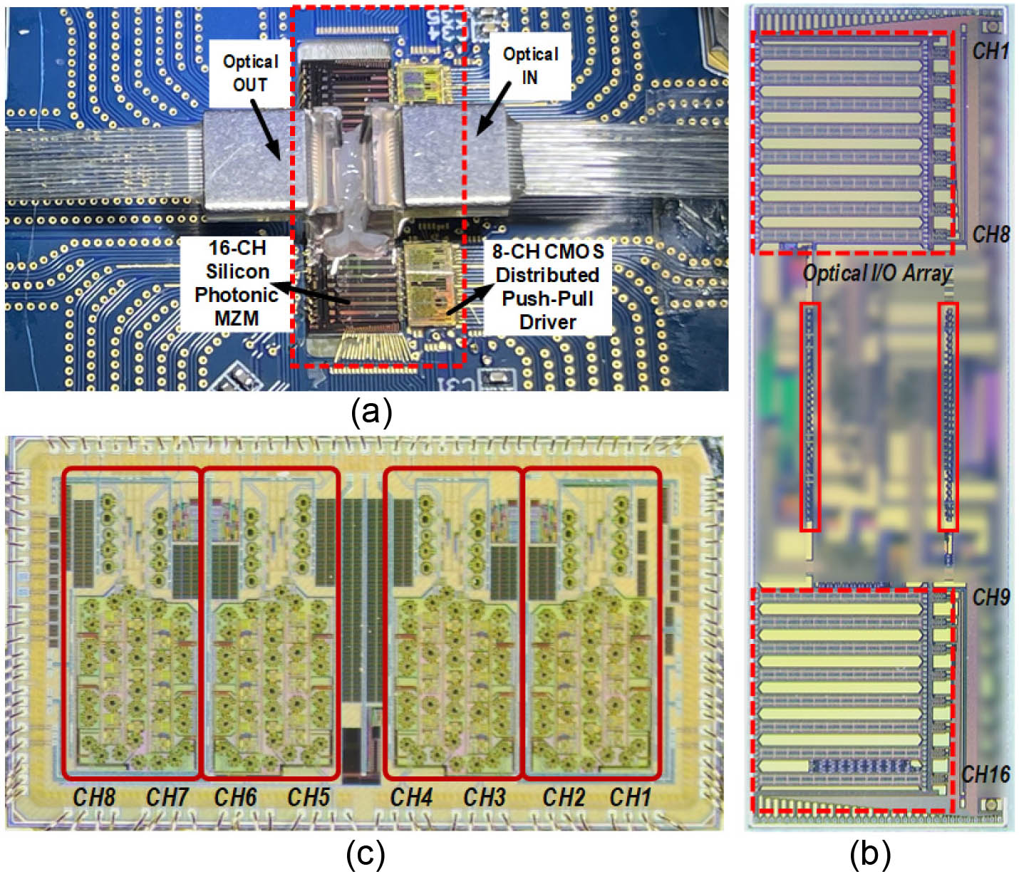
Figure 1.Proposed SiPh transmitter: (a) hybrid integration; (b) 16-CH MZM; and (c) 8-CH CMOS driver.
The SiPh integrated chip with arrayed MZMs is fabricated on a high-resistance silicon-on-insulator (SOI) wafer with a 220 nm thick silicon layer and a 2 μm thick buried oxide (BOX) using the foundry-ready CMOS process. The PN junction within the silicon MZM is fabricated with a doping concentrations of
![]()
Figure 2.(a) Cross section structure of the SiPh modulator arms. (b) EO bandwidth of the modulator.
The normalized S21 curves of the silicon modulator in 16-channel PICs under different bias voltages are plotted in Fig. 2(b). It is obvious that the modulator achieves an EO 3 dB bandwidth of
To optimize the hybrid integration, the driver employs a combination of a distributed amplifier (DA) architecture and push–pull topology, where the latter consumes no static power and the former extends the bandwidth significantly by absorbing the huge parasitic capacitance introduced by the CMOS transistors. As plotted in Fig. 3(a), the proposed EIC consists of a continuous-time linear equalizer (CTLE), a two-stage current-mode logical (CML) pre-driver, and a three-segment distributed push–pull driver.
![]()
Figure 3.Proposed distributed CMOS driver: (a) driver architecture; (b) two-tap FFE; and (c) push–pull driver cell.
The CTLE is located next to the input pad to compensate the bandwidth degradation caused by the channel loss, connectors, coaxial cables, and the parasitic capacitance of the electrostatic discharge (ESD) and the pads, providing a reconfigurable gain boosting at high frequency. The CTLE offers a 4-bit with a low-frequency gain range of 12 dB. Moreover, the input impedance is designed to
The differential signals after passing through the CTLE are amplified by a two-stage CML pre-driver to gain sufficient swing, and achieve an appropriate common-mode voltage shift for the following stage.
In the proposed EICs, a three-segment distributed architecture is employed, where a differential pair of a high-speed transmission line (T-line) and a push–pull driver cell is implemented into each segment. The input and output T-lines are designed with different characteristic impedances to provide terminations at both sides. To keep the same propagation velocity in the two T-lines, we intentionally adopted a lower characteristic impedance at the input, which helps to reduce the required inductance.
Due to a concern about the integration cost, the hybrid integration is realized through wire bonding, instead of extremely expensive 3D integration, such as chip-on-wafer-on-substrate (CoWoS) or integrated fan-out (InFO) packaging technology. Moreover, because the 16 channels are directly connected between the PIC and EIC chiplets, the differential data propagates longer traces on the printed circuit board (PCB), which is unavoidably more lossy than recently reported transmitters [29,37–41]. Consequently, between each segment, a specially developed FFE with a T-line-assisted two-tap is inserted to compensate for the insufficient bandwidth introduced by the CMOS mature process node, low-cost integration approach, and large channel scale. The merit of the proposed FFE technique is that it saves partial power dissipation of the delay cell and makes the push–pull output stages reconfigurable. The main path and FFE path constitute a segment in the distributed structure, and the currents are gathered at the output node.
The EIC and PIC are realized using a collaborative principle that aims for high integration density where the chiplets are set to be mutually agreeable; for example, the MZM can be directly driven and biased by the drivers without any off-chip bias tee. Furthermore, a push–pull cell is a good choice to efficiently drive long or large-capacitance SiPh MZMs, which are less sensitive to reflections.
3. INTEGRATED TRANSMITTER CHARACTERIZATION
The proposed eight-channel drivers are fabricated in a standard 65 nm CMOS process, occupying a chip size of
A. Electrical Behavior Measurement
A high-speed evaluation board (EVB) with well-matched differential T-lines is fabricated for the electrical behavior characterization, where the proposed driver is placed at the center and wire-bonded to establish connections to the equipment via coaxial cables, adaptors, and RF connectors. To obtain the frequency response, a broadband Keysight vector network analyzer (VNA) is used to characterize its gain, bandwidth, and terminal impedance. The measured S-parameter behavior in Figs. 4(a) and 4(b) indicates a good impedance matching of 50 Ω among the chip, instrument, and PCB trace; moreover, the absorption of additional parasitic capacitance can be observed. The discontinuous impedances are probably introduced by a bending of the test cables as well as the imperfect connections between cables and connectors. As shown in Fig. 4(c), good consistency is obtained among all eight channels, demonstrating an average bandwidth of 28 GHz, when the embedded CTLE and FFE are enabled.
![]()
Figure 4.Measured frequency response of proposed driver: (a) S11; (b) S22; and (c) S21.
In transient behavior evaluation, the EVB is assessed by feeding a differential pseudorandom binary sequence signal from a BPG in an OOK pattern. The outputs are connected to a high-speed sampling oscilloscope with two 6 dB attenuators. Figures 5(a) and 5(b) are the output NRZ-OOK eye diagrams at 32 Gb/s under different configurations, illustrating the effectiveness of FFE to compensate the nonlinearity and bandwidth insufficiency. At 50 Gb/s, the measured clear and open eye diagrams of the selected channels (1,3,5,7) are plotted in Figs. 4(c)–4(f), where rms jitters are 2.01 ps, 1.91 ps, 2.4 ps, and 1.93 ps, respectively. In addition, after 6 dB attenuation, the measured eye height is about 750 mV, including an extra 2–3 dB insertion loss added by PCB traces, adaptors, and cables. Thus, the effective differential output swing of the driver can be derived up to 4.0Vpp.
![]()
Figure 5.Measured electrical eye diagrams: (a) 32 Gb/s, FFE disabled; (b) 32 Gb/s, FFE enabled; (c) 50 Gb/s, Channel 1; (d) 50 Gb/s, Channel 3; (e) 50 Gb/s, Channel 5; and (f) 50 Gb/s, Channel 7.
B. Optical Performance Characterization
In optical performance characterization, hybrid integration of photonic chip and CMOS drivers is implemented by putting the chiplets on an optical evaluation board (OEVB). The experimental setup used for the measurement at various data rates is shown in Fig. 6. A tunable laser was used to generate cw at 1550 nm with 14 dBm output power. A commercial erbium-doped fiber amplifier is inserted between the transmitter and oscilloscope to compensate the optical loss from the MZM. In this test, every channel of the driver has
![]()
Figure 6.Experimental setup of the optical characterization. EDFA, erbium-doped fiber amplifier; and PRBS, pseudorandom binary sequence.
Figure 7(a) is the measured eye diagram at 32 Gb/s with no FFE equalization. As shown here, the insufficient bandwidth of the driver has a significant negative effect on the quality of eye diagram. After activating the equalization, the measured eye diagram under the same configuration and data rate is shown in Fig. 7(b), demonstrating the fact that two-tap FFE can effectively enhance the rising and falling edge speed, achieving a significant performance improvement. Figures 7(c)–7(f) are the eye diagrams of four randomly selected channels, indicating clear eye openings and successful transmission at 50 Gb/s with ER values of 3.36 dB, 3.27 dB, 3.81 dB, and 3.34 dB, with rms jitters around 3.0 ps, 3.0 ps, 2.0 ps, and 2.5 ps, respectively.
![]()
Figure 7.Measured optical eye diagrams: (a) 32 Gb/s, FFE disabled; (b) 32 Gb/s, FFE enabled; (c) 50 Gb/s, Channel 1; (d) 50 Gb/s, Channel 3; (e) 50 Gb/s, Channel 5; and (f) 50 Gb/s, Channel 7.
The duty cycle distortion seen in Fig. 7 mainly comes from the MZM, in which the phase shifters are constructed by reverse-biased P/N junctions. When the transient voltage applies changes, the modulator presents different capacitance to the driver, which in turn leads to an asymmetric rising and falling time.
4. DISCUSSION
Table 1 gives the performance summary and comparison to the recently reported state-of-the-art integrated optical transmitter. Due to the employment of a distributed structure, push–pull topology, and a two-tap FFE, the proposed SiPh transmitter achieves a higher data rate and larger swing under the same process node [38]. As shown in Table 1 and, to the best of our knowledge, 5.35 pJ/bit is one of lowest energy efficiencies in NRZ-OOK or other high-order pattern formats for a multichannel photonic–electric transmitter. A revised co-designed driver based on an advanced technology process is promising to bring the transmission speed and energy efficiency to a more optimized level.
Performance Summary and Comparison of SiPh Transmitter
| Transmitter | Laser | Signal | Channel | Swing | Data Rate | EIC | Power | Efficiency |
|---|---|---|---|---|---|---|---|---|
| SiPh MRM [ | O | PAM4 | 1 | 3.0 | 112 | 28 nm CMOS | 676 | 6.0 |
| SiPh MZM [ | O | PAM4 | 4 | – | 53.15 | 55 nm BiCMOS | 290 | 5.46 |
| SiPh MZM [ | O | NRZ | 1 | 2.5 | 25 | 65 nm CMOS | 275 | 11.0 |
| SiPh MZM [ | O | PAM4 | 1 | – | 56 | 55 nm BiCMOS | 300 | 5.36 |
| SiPh MZM [ | O | NRZ/PAM4 | 2 | 4.0 | 56 | 130 nm BiCMOS | 593 | 10.6 |
| SiPh MZM [ | – | NRZ/PAM4 | 1 | 1.8 | 56 | 16 nm CMOS | 708 | 12.6 |
| SiPh MZM [ | C | PAM4 | 4 | – | 200 | – | – | – |
| SiPh MZM [ | C | PAM4 | 2 | 4.0 | 50 | 40 nm CMOS | 1340 | 26.8 |
| SiPh MZM [ | C | NRZ | 1 | – | 100 | 28 nm CMOS | 203 | 2.03 |
| SiPh MZM (This work) | C | NRZ | 16 | 4.0 | 50 | 65 nm CMOS | 267.6 | 5.35 |
Excluding 160 mW on-chip laser power.
Including power dissipation of PAM4 CDR.
It is true that the proposed 16-channel photonic–electric co-designed silicon transmitter also suffers from crosstalk issues. We benchmark the crosstalk influence by testing the SNR of the eye diagram. As a result, the SNR is 5.49 dB and 6.25 dB, respectively, for a channel with an adjacent channel that is active or not. This drop will cause an approximately 10% decrease in the output driving voltage. In our case, the original output swing is 4Vpp, which exceeds the linear region of a silicon modulator even if considering a 10% reduction in peak-to-peak voltage. This electrical crosstalk induced degradation can hardly affect the optical signals. The tested SNR of an optical signal with or without an adjacent channel transmitting a signal varies within only 0.1 dB. The crosstalk, the reflection, and the bandwidth degradation are mainly caused by the large inductance of the bonding wire. Better performance can be realized in 3D integration [42]; however, the advanced electro-optical packaging is extremely expensive.
In conclusion, this work demonstrates an optical transmitter that only consumes 267.6 mW with an E/O conversion speed up to 50 Gb/s, achieving an output swing of
References
[3] N. Savage. Linking with light high-speed optical interconnects. IEEE Spectr., 39, 32-36(2002).
[8] K. Bergman. Photonic networks for intra-chip, inter-chip, and box-to-box interconnects in high performance computing. European Conference on Optical Communication, Tu1.2.1(2006).
[15] N. Kirman, M. Kirman, R. K. Dokania, J. F. Martinez, A. B. Apsel, M. A. Watkins, D. H. Albonesi. Leveraging optical technology in future bus-based chip multiprocessors. 39th Annual IEEE/ACM International Symposium on Microarchitecture, 492-503(2006).
[18] M. A. Taubenblatt. Optical interconnects for high-performance computing. J. Lightwave Technol., 30, 448-457(2012).
[19] R. Beausoleil, J. Ahn, N. Binkert, A. Davis, D. Fattal, M. Fiorentino, N. Jouppi, M. McLaren, C. Santori, R. Schreiber, S. Spillane, D. Vantrease, Q. Xu. A nanophotonic interconnect for high-performance many-core computation. 16th IEEE Symposium on High-Performance Interconnects, 182-189(2008).
[21] R. Meade, S. Ardalan, M. Davenport, J. Fini, C. Sun, M. Wade, A. Gladstein, C. Zhang. TeraPHY: a high-density electronic-photonic chiplet for optical I/O from a multi-chip module. Optical Fiber Communications Conference and Exhibition (OFC), M4D.7(2019).
[22] D. Kuchta, J. Proesel, F. Doany, W. Lee, T. Dickson, H. Ainspan, M. Meghelli, P. Pepeljugoski, X. Gu, M. Beakes, M. Schultz, M. Taubenblatt, P. Fortier, C. Dufort, E. Turcotte, M.-O. Pion, C. Bureau, F. Flens, G. Light, B. Trekell, K. Koski. Multi-wavelength optical transceivers integrated on node (MOTION). Optical Fiber Communications Conference and Exhibition (OFC), M4D.6(2019).
[23] G. Denoyer, A. Chen, B. Park, Y. Zhou, A. Santipo, R. Russo. Hybrid silicon photonic circuits and transceiver for 56 Gb/s NRZ 2.2 km transmission over single mode fiber. European Conference on Optical Communication (ECOC), 1-3(2014).
[24] Y. Ma, C. Williams, M. Ahmed, A. Elmoznine, D. Lim, Y. Liu, R. Shi, T. Huynh, J. Roman, A. Ahmed, L. Vera, Y. Chen, A. Horth, H. Guan, K. Padmaraju, M. Streshinsky, A. Novack, R. Sukkar, R. Younce, A. Rylyakov, D. Scordo, M. Hochberg. An all-silicon transmitter with co-designed modulator and DC-coupled driver. Optical Fiber Communication Conference (OFC), Tu2A.2(2019).
[26] H. Li, G. Balamurugan, M. Sakib, R. Kumar, H. Jayatilleka, H. Rong, J. Jaussi, B. Casper. A 3D-integrated microring-based 112 Gb/s PAM-4 silicon-photonic transmitter with integrated nonlinear equalization and thermal control. IEEE International Solid- State Circuits Conference (ISSCC), 208-210(2020).
[30] E. Temporiti, G. Minoia, M. Repossi, D. Baldi, A. Ghilioni, F. Svelto. A 56 Gb/s 300 mW silicon-photonics transmitter in 3D-integrated PIC25G and 55 nm BiCMOS technologies. IEEE International Solid-State Circuits Conference (ISSCC), 404-405(2016).
[31] L. Chen, C. Doerr, P. Dong, Y. Chen. Monolithic silicon chip with 10 modulator channels at 25 Gbps and 100-GHz spacing. Opt. Express, 19, B946-B951(2011).
[32] K. Li, D. Thomson, S. Liu, F. Meng, A. Shakoor, A. Khokhar, W. Cao, W. Zhang, P. Wilson, G. Reed. Co-design of electronics and photonics components for silicon photonics transmitters. European Conference on Optical Communication (ECOC), 1-3(2018).
[37] E. Sentieri, T. Copani, A. Paganini, M. Traldi, A. Palladino, A. Santipo, L. Gerosa, M. Repossi, G. Catrini, M. Campo, F. Radice, A. Diodato, R. Pelleriti, D. Baldi, L. Tarantini, L. Maggi, G. Radaelli, S. Cervini, F. Clerici, A. Moroni. A 4-channel 200 Gb/s PAM-4 BiCMOS transceiver with silicon photonics front-ends for gigabit ethernet applications. IEEE International Solid-State Circuits Conference (ISSCC), 210-212(2020).
[38] M. Cignoli, G. Minoia, M. Repossi, D. Baldi, A. Ghilioni, E. Temporiti, F. Svelto. A 1310 nm 3D-integrated silicon photonics Mach-Zehnder-based transmitter with 275 mW multistage CMOS driver achieving 6 dB extinction ratio at 25 Gb/s. IEEE International Solid-State Circuits Conference (ISSCC), 416-417(2015).
[39] E. Temporiti, G. Minoia, M. Repossi, D. Baldi, A. Ghilioni, F. Svelto. A 56 Gb/s 300 mW silicon-photonics transmitter in 3D-integrated PIC25G and 55 nm BiCMOS technologies. IEEE International Solid-State Circuits Conference (ISSCC), 404-405(2016).
[41] C. Li, K. Yu, J. Rhim, K. Zhu, N. Qi, M. Fiorentino, T. Pinguet, M. Peterson, V. Saxena, S. Palermo. A 3D-integrated 56 Gb/s NRZ/PAM4 reconfigurable segmented Mach-Zehnder modulator-based Si-photonics transmitter. IEEE BiCMOS and Compound Semiconductor Integrated Circuits and Technology Symposium (BCICTS), 32-35(2018).


Set citation alerts for the article
Please enter your email address

© Copyright 2018-2021 | Chinese Laser Press. All Rights Reserved 沪ICP备15018463号-20