Jianlu Wang. A novel spin-FET based on 2D antiferromagnet[J]. Journal of Semiconductors, 2019, 40(2): 020401
Search by keywords or author
- Journal of Semiconductors
- Vol. 40, Issue 2, 020401 (2019)
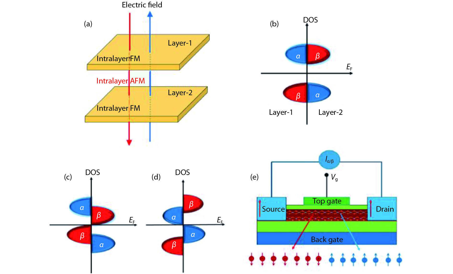
![(Color online) (a) Schematic view of the A-type antiferromagnetic bilayer system with the perpendicular electric field shown in blue (positve) and red (negative). (b−d) The schematic spin- and layer-resolved density of states of the A-type antiferromagnetic bilayer system with the electric field normal to the van der Waals plane (b) E = 0 and (c) (d) E = Ec (Ec is the critical electric field for the emergence of half metallicity), in which 1-α(β) and 2-α(β) indicate the spin-α(β) channel in layer 1 and layer 2, respectively. The positive(negative) electric field induces the spin-α(β) electrons around the Fermi level. (e) The proposed spin field effect transistor model, in which the spin states in the channel are tuned by the gate voltage[2].](/richHtml/jos/2019/40/2/020401/img_1.jpg)
Fig. 1. (Color online) (a) Schematic view of the A-type antiferromagnetic bilayer system with the perpendicular electric field shown in blue (positve) and red (negative). (b−d) The schematic spin- and layer-resolved density of states of the A-type antiferromagnetic bilayer system with the electric field normal to the van der Waals plane (b) E = 0 and (c) (d) E = E c (E c is the critical electric field for the emergence of half metallicity), in which 1-α (β ) and 2-α (β ) indicate the spin-α (β ) channel in layer 1 and layer 2, respectively. The positive(negative) electric field induces the spin-α (β ) electrons around the Fermi level. (e) The proposed spin field effect transistor model, in which the spin states in the channel are tuned by the gate voltage[2 ].

Set citation alerts for the article
Please enter your email address


