Engineering the electronic band structure of material systems enables the unprecedented exploration of new physical properties that are absent in natural or as-synthetic materials. Electronic structures of bilayer two-dimensional (2D) systems can be flexibly engineered by the external electric field. For example, the external electric field can open a band gap about 0.25 eV for the semimetal bilayer graphene, while in the bilayer transition metal dichalcogenides MX2 (M = Mo, W; X = S, Se, Te), the electric field can reduce the band gap and induce a semiconductor−metal phase transition. In 2017, the 2D ferromagnetic material Cr2Ge2Te6 has been confirmed in experiments, which stimulated the great research interest in 2D magnetic materials[1]. However, most of the reported 2D magnetic materials are antiferromagnets, which hinders their potential applications in spintronics.
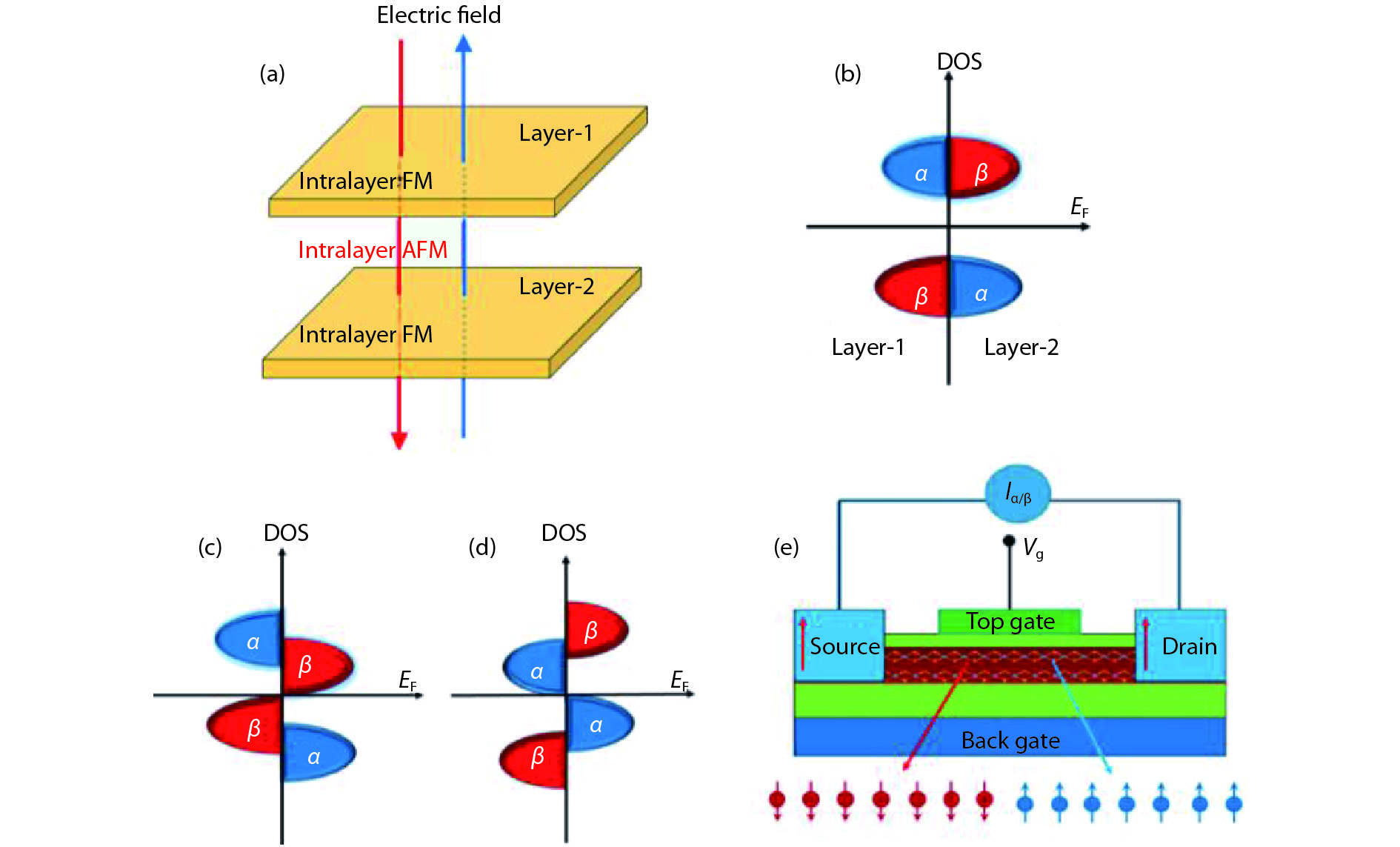
Fortunately, the recent research found that semiconducting bilayer A-type antiferromagnetic (intralayer ferromagnetic, interlayer antiferro-magnetic) can be made half metallic by applying the vertical electric field[2]. Half metallicity, an intriguing physical property arising from the metallic nature of electrons with singular spin polarization and insulating for oppositely polarized electrons, holds a great potential for a 100% spin-polarized current for high-efficiency spintronics. Fig. 1(a) shows the schematic structure of a semiconducting bilayer A-type antiferromagnetic, whose density of states is shown in Fig. 1(b). Under the applied electric field, the electrostatic potential of one constituent layer rises and that of the other layer decreases, resulting in a semiconductor−metal phase transition, shown in Figs. 1(c) and 1(d). The blue (positive) and red (negative) electric fields shown in Fig. 1(a) result in the electronic structures in Figs. 1(d) and 1(c), respectively. The most interesting finding is that the electric field induced metal states are from one spin channel, i.e., we achieve the half-metallicity in the 2D antiferromagnet by an all-electric method.
![(Color online) (a) Schematic view of the A-type antiferromagnetic bilayer system with the perpendicular electric field shown in blue (positve) and red (negative). (b−d) The schematic spin- and layer-resolved density of states of the A-type antiferromagnetic bilayer system with the electric field normal to the van der Waals plane (b) E = 0 and (c) (d) E = Ec (Ec is the critical electric field for the emergence of half metallicity), in which 1-α(β) and 2-α(β) indicate the spin-α(β) channel in layer 1 and layer 2, respectively. The positive(negative) electric field induces the spin-α(β) electrons around the Fermi level. (e) The proposed spin field effect transistor model, in which the spin states in the channel are tuned by the gate voltage[2].](/Images/icon/loading.gif)
Figure 1.(Color online) (a) Schematic view of the A-type antiferromagnetic bilayer system with the perpendicular electric field shown in blue (positve) and red (negative). (b−d) The schematic spin- and layer-resolved density of states of the A-type antiferromagnetic bilayer system with the electric field normal to the van der Waals plane (b) E = 0 and (c) (d) E = Ec (Ec is the critical electric field for the emergence of half metallicity), in which 1-α(β) and 2-α(β) indicate the spin-α(β) channel in layer 1 and layer 2, respectively. The positive(negative) electric field induces the spin-α(β) electrons around the Fermi level. (e) The proposed spin field effect transistor model, in which the spin states in the channel are tuned by the gate voltage[2].
A novel the spin field effect transistor (Spin-FET) has been proposed based on the half-metallicity in the bilayer A-type antiferromagnetic system [Fig. 1(e)]. When the external electric field exceeds the critical electric field Ec, electrons with 100% spin polarization can be generated, and the spin states in the transport channel can be switched between spin-α and spin-β by reversing the direction of the applied electric field. In 1990, Datta and Das proposed the well-known Spin-FET, whose performance depends on the precise control of the spin precession in the transport channel based on Rashba spin orbit coupling (SOC)[3]. Although Datta-Das Spin-FET wins the constant research interest in the past several decades, many difficulties are involved in the device and yet to be solved, for example, strong Rashba SOC is required to tune the spin precession, which simultaneously brings the serious spin decoherence effect. In the 2D antiferromagnet, the electric field engineers the band structure of A-type antiferromagnet, flexibly switching the electron spin between α and β states. The method is simple, convenient, and innovative, which is completely different from the Datta-Das spin field effect transistor.
References
[1] C Gong, L Li, Z Li et al. Discovery of intrinsic ferromagnetism in two-dimensional vander Waals crystals. Nature, 546, 265(2017).
[2] S Gong, C Gong, Y Sun et al. Electrically induced 2D half-metallic antiferromagnets and spin field effect transistors. PNAS, 115, 8511(2018).
[3] S Datta, B Das. Electronic analog of the electro-optic modulator. Appl Phys Lett, 56, 655(1990).