Abstract
The emergence of light-tunable synaptic transistors provides opportunities to break through the von Neumann bottleneck and enable neuromorphic computing. Herein, a multifunctional synaptic transistor is constructed by using 2,7-dioctyl[1]benzothieno[3,2-b][1]benzothiophene (C8-BTBT) and indium gallium arsenide (InGaAs) nanowires (NWs) hybrid heterojunction thin film as the active layer. Under illumination, the Type-I C8-BTBT/InGaAs NWs heterojunction would make the dissociated photogenerated excitons more difficult to recombine. The persistent photoconductivity caused by charge trapping can then be used to mimic photosynaptic behaviors, including excitatory postsynaptic current, long/short-term memory and Pavlovian learning. Furthermore, a high classification accuracy of 89.72% can be achieved through the single-layer-perceptron hardware-based neural network built from C8-BTBT/InGaAs NWs synaptic transistors. Thus, this work could provide new insights into the fabrication of high-performance optoelectronic synaptic devices.The emergence of light-tunable synaptic transistors provides opportunities to break through the von Neumann bottleneck and enable neuromorphic computing. Herein, a multifunctional synaptic transistor is constructed by using 2,7-dioctyl[1]benzothieno[3,2-b][1]benzothiophene (C8-BTBT) and indium gallium arsenide (InGaAs) nanowires (NWs) hybrid heterojunction thin film as the active layer. Under illumination, the Type-I C8-BTBT/InGaAs NWs heterojunction would make the dissociated photogenerated excitons more difficult to recombine. The persistent photoconductivity caused by charge trapping can then be used to mimic photosynaptic behaviors, including excitatory postsynaptic current, long/short-term memory and Pavlovian learning. Furthermore, a high classification accuracy of 89.72% can be achieved through the single-layer-perceptron hardware-based neural network built from C8-BTBT/InGaAs NWs synaptic transistors. Thus, this work could provide new insights into the fabrication of high-performance optoelectronic synaptic devices.Introduction
With the clipping evolution of artificial intelligence systems, massive amounts of data now need to be processed efficiently[1-5]. However, traditional computers with von Neumann architecture are frequently unable to process unstructured information[6-11]. The achievement of synaptic functions can supply the elementary information processing unit for the coming neural network computer, enlightened by the human brain[12-16]. Up to now, phase-change memory and memristors are particularly well-reported, where synaptic devices can be effectively stimulated by electrical signals[17-21]. But for the light signals, it can provide low consumption stimulation, high bandwidth, strong anti-interference ability, high energy efficiency and ultra-fast signal transmission[22-25].
Recently, light-stimulated synaptic devices have attracted significant attention[26,27]. Hanet al. fabricated an organic photoelectric synaptic transistor (PST) by using quantum dots and 2D materials with polymers as the hybrid photoactive dielectric layer[28]. Besides, Huanget al. demonstrated a transistor constructed based on the blending of biomaterials and organic semiconductor materials[29]. These works revealed the considerable application potential of hybrid materials in PST. It is noted that indium gallium arsenide (InGaAs) is a typical III–V alloy semiconductor with a narrow bandgap at room temperature[10], high electron mobility, large quantum efficiency, low leakage current and strong radiation resistance, which is widely used in the fabrication of electronic and optoelectronic devices[30]. Moreover, the 2,7-dioctyl[1]benzothieno[3,2-b][1]benzothiophene (C8-BTBT) as a promising organic semiconductor has advantages in high crystallinity[31], efficient charge transport and high ultraviolet responsivity[32-34]. The combination of these two materials would provide effective tactics for manufacturing photoelectric devices.
In this work, a multifunctional PSTs were fabricated using hybrid C8-BTBT/InGaAs NWs heterojunction thin films as the active layers. These devices successfully mimicked human synaptic behaviors, including excitatory postsynaptic current (EPSC), paired-pulse facilitation (PPF) and Pavlovian conditioning. Then, we demonstrate the applicability of the C8-BTBT/InGaAs NWs synaptic transistors in building high-performance neuromorphic networks using a single-layer-perceptron hardware-based neural network (SLP HW-NN) for the Modified National Institute of Standards and Technology (MNIST) handwritten digit dataset with a recognition accuracy as high as 89.72%.
Experimental section
InGaAs nanowires preparation
InGaAs nanowires were synthesized on Si/SiO2 wafer pieces (270 nm thick thermally grown oxide) in a two-zone horizontal tube furnace using a chemical vapor transport method. The mixed InAs and GaAs powders (with the ratio of 1 : 9 in wt%) were loaded into a boron nitride crucible at the upstream zone of the furnace. The growth substrate pre-deposited with a 0.5 nm thick (nominal thickness) Au film as the catalyst was set at the downstream zone. The temperature of the downstream zone was first elevated to 800 °C and kept for 10 min in order to anneal the Au catalyst. Then, the temperature of the downstream zone was cooled directly to the growth temperature (660 °C) for the first step growth and the source temperature was started to elevate at the same time. When the source temperature reached the designated value (810 °C), the first nucleation step began. After 1−2 min, the downstream was stopped with the heating and then cooled to a second step growth temperature (570 °C). Finally, the second step growth lasted for 40 minutes. The hydrogen (99.9995%) was used as a carrier gas during the entire growth process with the flowrate maintained at 100 sccm.
Materials and devices fabrication
2,7-dioctyl[1]benzothieno[3,2-b][1]benzothiophene (C8-BTBT) was purchased from SunaTech Inc. without further purification. Polystyrene (PS) was purchased from Sigma-Aldrich without further purification.
Methods
A heavily n-doped Si wafer with a thermally grown SiO2 layer (285 nm) was used as the substrate. Before device preparation, the substrate was sonicated in acetone and ethanol for 30 min, respectively, then rinsed with isopropanol, and finally dried by N2. Next, the substrate was modified under UV ozone for 20 min. During the off-center spin coating (OCSC) process, C8-BTBT was dissolved in chlorobenzene (CB) with a concentration of 5 mg/mL. PS was added into the C8-BTBT solution as an additive (10 wt% of PS). The substrate prepared with the nanowires was put into the chlorobenzene solution, sonicated for 5 s, and then 200 mL of the solution was taken out and mixed with the C8-BTBT solution to form a ternary solution. The semiconductor layer was fabricated on the SiO2 via the same OCSC process in the N2-golve box. Finally, 50-nm-thick Ag source and drain electrodes were deposited at a pressure of ~8 × 10⁻⁴ Pa on C8-BTBT films with a shadow mask, resulting in a channel with length-to-width ratio of 80μm/1000μm.
Characterization
The electrical properties and synaptic function of the prepared C8-BTBT/InGaAs NWs transistors were measured in a shielded box using a semiconductor parameter analyzer (Keithley 4200-SCS). All data were measured in air with a relative humidity of 28%.
Results and discussion
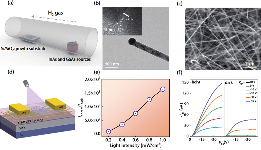
The two-step catalytic solid-source chemical vapor deposition (CVD) was utilized to synthesize InGaAs NWs[30].Fig. 1(a) shows a schematic illustration of the CVD step up for the NWs synthesis. The high-resolution transmission electron microscope (HRTEM) and scanning electron microscope (SEM) are adopted to characterize the physical features of InGaAs NWs. The HRTEM and SEM images are shown inFigs. 1(b) and1(c), exhibiting the straight and uniform nanowire with the 3.5 Å of inter planar spacing, which is in line with the <111> prominent direction of NWs. Subsequently, the energy dispersive spectrometer (EDS) mapping of TEM is used to show the uniform distribution of In, Ga and As elements along the NWs (Fig. S1).

Figure 1.(Color online) (a) Schematic illustration of the CVD setup for the NWs synthesis. (b) SEM image and (c) HRTEM image of the InGaAs NWs. (d) Device schematic of the C8-BTBT/InGaAs NWs phototransistors. (e)Ilight/Idark curve from the devices under light with different intensities. (f) Output characteristics in dark and under light (0.4 mW/cm2).
The composition of InGaAs NWs is confirmed by EDS shown in Figs. S2(a) and S2(b), which determines the composition of InxGa1–xAs withx being about 0.43. Fig. S2(c) exhibits a SEM image of a cross-section of a C8-BTBT/InGaAs NWs heterojunction prepared on a silicon substrate with SiO2 dielectric layer (285 nm), which shows that the thickness of the active layer is approximately 40 nm. Next, the X-ray photoelectron spectroscopy (XPS) image of the thin film added with NWs is shown in Fig. S2(d). A slight peak shift of S 2p into the lower binding energy shows the carrier transfer between the C8-BTBT and InGaAs NWs. Then,Fig. 1(d) shows the schematic diagram of an artificial synaptic device based on hybrid organic-inorganic heterojunction. The relationship betweenIphoto/Idark ratio and light intensity is investigated and shown inFig. 1(e). When the gate-source voltage (Vgs) is 20 V, the incident light intensity is 0.2 mW/cm2, and theIphoto/Idark ratio of the device reaches 2.7 × 10⁷. Fig. S3(a) is an atomic force microscope (AFM) image of a C8-BTBT/InGaAs NWs hybrid thin film, demonstrating the film hold slick surface and low roughness with the root-mean-square roughness (RMS) is 0.64 nm. The AFM image of C8-BTBT thin film is also shown in Fig. S3(b). Moreover, Fig. S3(c) shows the transfer curves of the devices that are exposed to different illumination intensities and gate voltages. It is evident that the higherIphoto/Idark ratio can be achieved by boosting the light power. The output curves of the device are also essential to evaluate the photoresponse performance. When exposed to the light of 0.4 mW/cm2, the drain-source current (Ids) of the device increases significantly under all differentVgs, which shown inFig. 1(f). When theVgs is –10 V, the device completely shut down in the dark. The minimum device current can reach –1.0 × 10⁻¹⁴ A, and the overall level is maintained at about –9.5 × 10⁻¹⁴ A. Under light irradiation,Ids can increase to –51µA significantly.
The formation of memory in the brain is relevant to the establishment of a synapse.Fig. 2(a) demonstrates the parts of the brain related to memory and schematic diagrams of biological synapses. The designed synaptic devices based on organic-inorganic hybrid film realize the slow current decay, which can be used to mimic synaptic-like behaviors[35,36]. To understand the importance of NWs in synaptic devices, only C8-BTBT:PS is deposited as the reference.Fig. 2(b) shows a weak EPSC response of the C8-BTBT transistors. When applying a light pulse to the device (365 nm, 0.4 mW/cm2, 0.05 s), the EPSC immediately peaks up to –27 nA and then swiftly dives to 10.4% under dark condition. The electron–hole pairs in the C8-BTBT channel layer are generated after light irradiation, and the photo generated holes fractionally occupy the charge trap state at the C8-BTBT/SiO2 interface. When the light is turned off, the photo generated holes will gradually be recaptured, resulting in decreased EPSC behavior[37]. In contrast, the synaptic devices with hybrid C8-BTBT/InGaAs NWs film show a much stronger EPSC under the same light stimulation. When removing the light pulse, the device current dives to 43.0% (Fig. 2(c)), demonstrating significant non-volatility. The main reason for the apparent enhancement of synaptic behavior after adding the InGaAs NWs is that the InGaAs NWs play the role of a hole trap to prevent the recombination of photogenerated electrons in C8-BTBT[38]. Under the irradiation of light (light absorption of C8-BTBT and InGaAs NWs are shown in Figs. S4(a) and S4(b), respectively), C8-BTBT will cause the separation of electron-hole pairs and result in the improvement of carrier concentration. Meanwhile, the highest occupied molecular orbital (HOMO) and lowest occupied molecular orbital (LUMO) levels of C8-BTBT totally cover the conduction band (CB) and valence band (VB) of InGaAs NWs. Thus, the Type-I heterojunction is constructed, and it is beneficial to transfer holes from the C8-BTBT layer to InGaAs NWs under the light stimulation[39]. The (αhν)2–hν curves of C8-BTBT and InGaAs NWs are shown in Figs. S4(c) and S4(d), demonstrating a big difference in the band gap and confirming the Type-I heterojunction of organic-inorganic hybrid film. Moreover, the detailed process of carrier transport is shown in Fig. S5. On the one hand, under a negative electric field applied on the gate, a small part of photo-generated holes in C8-BTBT can be captured by interface defect. On the other hand, because of the relatively large gap and energy barrier between the LUMO level of C8-BTBT and CB of InGaAs NWs, the transfer of electrons from C8-BTBT to InGaAs NWs is more difficult than holes[40]. Therefore, the more photogenerated holes will be trapped by InGaAs NWs under light stimulation, which will leave the photogenerated electrons in C8-BTBT film and cause the persistent photocurrent.
Figure 2.(Color online) (a) Schematic illustration on the workings of brain connections and biological synapses. (b, c) EPSC stimulated by a light pulse for the phototransistors from pure C8-BTBT and C8-BTBT/InGaAs NWs transistors, respectively. (d) ΔW as a function of time collected from EPSC. (e, f) PPF measured from the phototransistors with pure C8-BTBT and C8-BTBT/InGaAs NWs transistors, respectively. (g) PPF index decay and fitting curves.
The change of synaptic weight (
is defined as
, of which
is the initial channel current andIp is the postsynaptic current changes over time after the light pulse. AsFig. 2(d) illustrated, the ∆W of the C8-BTBT/InGaAs NWs synaptic transistor is significantly larger than that of only C8-BTBT device. The results indicate that the organic-inorganic hybrid thin film could induce more carrier capture and retention, showing better potential in mimicking human synaptic behaviors. Hence, this behavior is used to simulate the learning-forgetting-relearning process by employing a pair of successive light pulses, as illustrated inFig. 2(e). The PPF index as an important neurological function is mimicked successfully by the PST. Here, the two consecutive peaks are applied with 300 ms time interval. The following formula can be used to describe the PPF index:
, where the first and second EPSC values are represented by A1 and A2, respectively[41]. It is obvious that when the organic-inorganic hybrid thin film is introduced, the more pronounced PPF index is realized with the same interval time (Fig. 2(f)).Fig. 2(g) compares the differences between the two devices in PPF index. According to the trend of the curve, PPF index of pure C8-BTBT devices is easier to decay to the initial current, while C8-BTBT/InGaAs NWs devices can maintain for a longer time. Compared with the C8-BTBT device, the C8-BTBT/InGaAs NWs hybrid thin film has more contact interfaces of organic and inorganic materials. Therefore, the photogenerated holes can be captured at the organic semiconductor-NWs interface and dielectric/organic semiconductor interface, offering a stronger carrier storage capacity.
Similarly, the artificial synaptic devices can also be converted from short-term plasticity (STP) to long-term plasticity (LTP) by using different number of light pulses, pulse widths, pulse intensities, and so on[6]. After the light pulses stimulation with varying power density, the EPSC are calculated by measuring the difference between current after spark 1 and 2 s (It) and resting current (I0) before pulse spark, which is shown inFig. 3(a). Similar toFig. 3(a),Fig. 3(b) shows the EPSC changed with different pulse widths. TheIt is measured at 1 and 2 s after stimulation with different pulse widths. The results suggest that the addition of NWs could make the dissociated excitons more difficult to recombine, and the channel decays more slowly at the same time.
Figure 3.(Color online) (a) Light intensity dependence of the EPSC with different light pulse stimulation. (b) Light pulse width dependence of the EPSC with different width stimulation. (c) The EPSC of 10 consistent light pulses measured from the different light intensity. (d) EPSC change extracted from (c). (e) Photonic potentiation and electric depression by 30 times of light pulses and negative electric pulses. (f) Stability testing of photoresponse of C8-BTBT/InGaAs NWs phototransistors.
Multi-level stimulus behavior with 10 continuous light pulses (0.4 mW/cm2, width = 0.2 s, interval = 1.8 s) are demonstrated inFig. 3(c). The conductivity state with many modulation stages is observed, indicating that the PST has the potential to achieve multi-level optical storage. Due to the augment of light stimulation intensity, the significant change of EPSC shows the tendency of transformation from STP to LTP. The behavior could be explained that as the intensity of light pulse increases and more holes are injected into the InGaAs NWs. Moreover, the increase in optical power density could realize a conversion for the device from STP to LTP.Fig. 3(d) is extracted fromFig. 3(c), demonstrating the connections between the EPSC, the number of pulses and different light power intensity. The long-time potentiation/depression characteristics of optoelectronic synaptic devices could be also confirmed for continuous light and voltage pulses, which are presented inFig. 3(e). The readout current increased stepwise under 30 optical stimuli (0.4 mW/cm2, width = 0.2 s, interval = 3.8 s). Then, under 30 electrical stimulations (–40 V, width = 0.2 s, interval = 3.8 s), the synaptic transistor shows a stepwise decreasing trend. Furthermore, the photoresponse of C8-BTBT/InGaAs NWs phototransistors can be turned on and off by light irradiation (0.08 mW/cm2, 49 s) and electrical pulse (–70 V and 2 s), respectively. Several work cycles of organic–inorganic artificial synapse based on PST are shown inFig. 3(f).
As discussed above, due to the relatively high light absorption of the thin film, multiple interfaces and Type-I band structure, the photogenerated holes can be easier to transfer and are trapped by the InGaAs NWs. As shown inFig. 4(a), the electrons left in organic semiconductor which cannot be recombined. Then the persistent photoconductivity is induced. At the same time, due to the position of the Fermi energy level, there is a potential barrier at the interface, which further hinders the electrons transfer and holes backflow. Besides, inFig. 4(b), a large voltage (–70 V) is applied to the gate to pull the trapped electrons from the InGaAs NWs and this results in the device returning to the off state quickly. Thus, the state of the devices can be switched through light stimulation and gate voltage repeatedly. Importantly, in order to investigate the potential in practice application, Pavlovian learning (classical conditioning) is demonstrated based on the PST[42]. As shown in theFig. 4(c), the electrical and light pulses could be adopted as conditioned stimulus and unconditioned stimulus, respectively. We define a threshold of 0.4μA. The 0.2 s continuous optical pulse simulates the initial food and induces the EPSC to reach the threshold. The initial bell ring is simulated with five consecutive electrical pulses, which does not induce the salivation response threshold simulation. After 0.2 s of continuous optical pulse and electrical pulse repetitive stimulation, EPSC over 0.4μA is observed, indicating the Pavlovian simulations reach the saliva threshold. The complete association process and human brain memory process are shown in the Fig. S6. It obviously shows that the mixing stimuli can realize the classical Pavlovian conditioning successfully and strengthen the effect of learning by increasing the learning times[43].
Figure 4.(Color online) Schematic illustrations of (a) the existence of electrons in the device after light illumination and (b) the recombination process of electrons and holes with voltage applied to the gate. (c) The complete association learning process. After training, CS can trigger UR (canine saliva secretion, unconditional response).
Finally, in order to illustrate the performance improvement of the C8-BTBT/InGaAs NWs synaptic transistor in neuromorphic computation, these PSTs with discrete and finite conductivity characteristics are used to construct a SLP HW-NN[44]. In PST, changes in channel conductance result in changes in synaptic weights. The long-term potentiation process is driven by 50 light pulses (0.4 mW/cm2, width = 0.2 s, interval = 3.8 s), while 50 voltage pulses drive the long-term depression process (–40 V, width = 0.2 s, interval = 3.8 s).Figs. 5(a) and5(b) show the corresponding mean values of the variation range for long-time potentiation/long-time depression characteristics in several C8-BTBT and C8-BTBT/InGaAs NWs transistors, respectively[45]. In order to make dynamic range more prominent and noticeable,Gmax/Gmin value is used for evaluation[46]. TheGmax/Gmin value of C8-BTBT transistors is 41.6, and the ratio of C8-BTBT/InGaAs NWs transistors is 197.2, which exhibits a more remarkable conductivity change, as described inFig. 5(c).
Figure 5.(Color online) (a) LTP/LTD characteristics of the C8-BTBT transistors. (b) LTP/LTD characteristics of the C8-BTBT/InGaAs NWs transistors. (c) Simulated neural network accuracy for MNIST handwritten digit classification for the C8-BTBT transistors (red) and the C8-BTBT/InGaAs NWs transistors (black). (d) Schematic of SLP HW-NN. (e) Corresponding hardware implementation composed of PST crossbar array. (f) Change of the recognition rate with epochs of training.
The performance of SLP HW-NN consisting of C8-BTBT and C8-BTBT/InGaAs NWs PST are evaluated, respectively. The 60 000 training sets are applied in the MNIST dataset for learning and 10 000 image test sets to assess classification precision. The MINIST dataset is composed of handwritten digital images with 10 classes (from 0 to 9) and each image is 28 × 28 pixels. Therefore, a SLP HW-NN consists of 784 input neurons and 10 output neurons, exhibited inFig. 5(d)[47]. Moreover,Fig. 5(e) presents the synaptic apparatus array corresponding to the SLP HW-NN. As shown inFig. 5(f), the simulation results indicate that the SLP HW-NN composed of C8-BTBT could provide up to 82.78% recognition rate. In contrast, the C8-BTBT/InGaAs NWs synaptic devices can provide a recognition accuracy as high as 89.72%. This demonstrates that the C8-BTBT/InGaAs NWs PST has more advantages in neural network classification recognition.
Conclusion
In summary, an efficient photo-synaptic transistor that is based on a C8-BTBT/InGaAs NWs hybrid heterojunction thin film is constructed. The addition of InGaAs NWs improves the retention of the continuous conductance and exhibits excellent photoresponse characteristics and programmable persistent photoconductivity effects to simulate basic biological synaptic behavior. The simulated SLP HW-NN composed of C8-BTBT/InGaAs NWs PST can achieve classification accuracy as high as 89.72% for MNIST dataset, which shows the great potential in practical application.
Appendix A. Supplementary materials
Supplementary materials to this article can be found online athttps://doi.org/10.1088/1674-4926/43/11/112201.
References
[1] T Ahmed, M Tahir, M X Low et al. Fully Light-controlled memory and neuromorphic computation in layered black phosphorus. Adv Mater, 33, 2004207(2021).
[2] Y X Hou, Y Li, Z C Zhang et al. Large-scale and flexible optical synapses for neuromorphic computing and integrated visible information sensing memory processing. ACS Nano, 15, 1497(2021).
[3] M Lee, M Kim, J W Jo et al. Suppression of persistent photo-conductance in solution-processed amorphous oxide thin-film transistors. Appl Phys Lett, 112, 052103(2018).
[4] M Lee, W Lee, S Choi et al. Brain-inspired photonic neuromorphic devices using photodynamic amorphous oxide semiconductors and their persistent photoconductivity. Adv Mater, 29, 1700951(2017).
[5] Z Lv, M Chen, F Qian et al. Mimicking neuroplasticity in a hybrid biopolymer transistor by dual modes modulation. Adv Funct Mater, 29, 1902374(2019).
[6] H Wang, Q Zhao, Z Ni et al. A ferroelectric/electrochemical modulated organic synapse for ultraflexible, artificial visual-perception system. Adv Mater, 30, 1803961(2018).
[7] X Wang, Y Lu, J Zhang et al. Highly sensitive artificial visual array using transistors based on porphyrins and semiconductors. Small, 17, 2005491(2021).
[8] D Xie, L Wei, M Xie et al. Photoelectric visual adaptation based on 0D-CsPbBr3-quantum-dots/2D-MoS2 mixed-dimensional heterojunction transistor. Adv Funct Mater, 31, 2010655(2021).
[9] L Q Zhu, C J Wan, L Q Guo et al. Artificial synapse network on inorganic proton conductor for neuromorphic systems. Nat Commun, 5, 1(2014).
[10] L F Abbott, r W G Regehr. Synaptic computation. Nature, 431, 796(2004).
[11] S H Sung, T J Kim, H Shin et al. Memory-centric neuromorphic computing for unstructured data processing. Nano Res, 14, 3126(2021).
[12] C Qian, L A Kong, J Yang et al. Multi-gate organic neuron transistors for spatiotemporal information processing. Appl Phys Lett, 110, 083302(2017).
[13] C J Wan, L Q Zhu, Y H Liu et al. Proton-conducting graphene oxide-coupled neuron transistors for brain-inspired cognitive systems. Adv Mater, 28, 3557(2016).
[14] C Han, X Han, J Han et al. Light-stimulated synaptic transistor with high PPF feature for artificial visual perception system application. Adv Funct Mater, 32, 2113053(2022).
[15] C Qian, Y Choi, Y J Choi et al. Oxygen-detecting synaptic device for realization of artificial autonomic nervous system for maintaining oxygen homeostasis. Adv Mater, 32, 2002653(2020).
[16] Y Jang, J Park, J Kang et al. Amorphous InGaZnO (a-IGZO) synaptic transistor for neuromorphic computing. ACS Appl Electron Mater, 4, 1427(2022).
[17] X Yan, J H Qian, V K Sangwan et al. Progress and challenges for memtransistors in neuromorphic circuits and systems. Adv Mater, 2108025(2022).
[18] W Huh, D Lee, C H Lee. Memristors based on 2D materials as an artificial synapse for neuromorphic electronics. Adv Mater, 32, 2002092(2020).
[19] J Shi, S D Ha, Y Zhou et al. A correlated nickelate synaptic transistor. Nat Commun, 4, 1(2013).
[20] M Suri, O Bichler, D Querlioz et al. Physical aspects of low power synapses based on phase change memory devices. J Appl Phys, 112, 054904(2012).
[21] H Shim, S Jang, J G Jang et al. Fully rubbery synaptic transistors made out of all-organic materials for elastic neurological electronic skin. Nano Res, 15, 758(2022).
[22] E Kuramochi, K Nozaki, A Shinya et al. Large-scale integration of wavelength-addressable all-optical memories on a photonic crystal chip. Nat Photonics, 8, 474(2014).
[23] Z Luo, Y Xie, Z Li et al. Plasmonically engineered light-matter interactions in Au-nanoparticle/MoS2 heterostructures for artificial optoelectronic synapse. Nano Res, 15, 3539(2022).
[24] L Qian, Y Sun, M Wu et al. A lead-free two-dimensional perovskite for a high-performance flexible photoconductor and a light-stimulated synaptic device. Nanoscale, 10, 6837(2018).
[25] Y Sun, L Qian, D Xie et al. Photoelectric synaptic plasticity realized by 2D perovskite. Adv Funct Mater, 29, 1902538(2019).
[26] S Wang, C Chen, Z Yu et al. A MoS2/PTCDA hybrid heterojunction synapse with efficient photoelectric dual modulation and versatility. Adv Mater, 31, 1806227(2019).
[27] S Qin, F Wang, Y Liu et al. A light-stimulated synaptic device based on graphene hybrid phototransistor. 2D Mater, 4, 035022(2017).
[28] Y Wang, J Yang, Z Wang et al. Near-infrared annihilation of conductive filaments in quasiplane MoSe2/Bi2Se3 nanosheets for mimicking heterosynaptic plasticity. Small, 15, 1805431(2019).
[29] B Yang, Y Lu, D Jiang et al. Bioinspired multifunctional organic transistors based on natural chlorophyll/organic semiconductors. Adv Mater, 32, 2001227(2020).
[30] J J Hou, F Wang, N Han et al. Stoichiometric effect on electrical, optical, and structural properties of composition-tunable InxGa1–xAs nanowires. ACS Nano, 6, 9320(2012).
[31] Y Huang, J Sun, J Zhang et al. Controllable thin-film morphology and structure for 2,7-dioctyl[1]benzothieno[3,2-b][1] benzothiophene (C8-BTBT) based organic field-effect transistors. Org Electron, 36, 73(2016).
[32] P Xie, T Liu, J Sun et al. Solution-processed ultra-flexible C8-BTBT organic thin-film transistors with the corrected mobility over 18 cm2/(V·s). Sci Bull, 65, 791(2020).
[33] S Tong, J Sun, C Wang et al. High-performance broadband perovskite photodetectors based on CH3NH3PbI3/C8-BTBT heterojunction. Adv Electron Mater, 3, 1700058(2017).
[34] Y Yuan, J Huang. Ultrahigh gain, low noise, ultraviolet photodetectors with highly aligned organic crystals. Adv Opt Mater, 4, 264(2016).
[35] A Mukherjee, S Sagar, S Parveen et al. Superionic rubidium silver iodide gated low voltage synaptic transistor. Appl Phys Lett, 119, 253502(2021).
[36] S Kim, B Choi, M Lim et al. Pattern recognition using carbon nanotube synaptic transistors with an adjustable weight update protocol. ACS Nano, 11, 2814(2017).
[37] S Dai, X Wu, D Liu et al. Light-stimulated synaptic devices utilizing interfacial effect of organic field-effect transistors. ACS Appl Mater Interfaces, 10, 21472(2018).
[38] J Han, J Wang, M Yang et al. Graphene/organic semiconductor heterojunction phototransistors with broadband and bi-directional photoresponse. Adv Mater, 30, 1804020(2018).
[39] H Xia, S Tong, C Zhang et al. Flexible and air-stable perovskite network photodetectors based on CH3NH3PbI3/C8-BTBT bulk heterojunction. Appl Phys Lett, 112, 233301(2018).
[40] D Yang, X Zhang, K Wang et al. Stable efficiency exceeding 20.6% for inverted perovskite solar cells through polymer-optimized PCBM electron-transport layers. Nano Lett, 19, 3313(2019).
[41] L Xu, H Xiong, Z Fu et al. High conductance margin for efficient neuromorphic computing enabled by stacking nonvolatile van der waals transistors. Phys Rev Appl, 16, 044049(2021).
[42] F Yu, L Q Zhu, H Xiao et al. Restickable oxide neuromorphic transistors with spike-timing-dependent plasticity and pavlovian associative learning activities. Adv Funct Mater, 28, 1804025(2018).
[43] Y B Guo, L Q Zhu, T Y Long et al. Bio-polysaccharide electrolyte gated photoelectric synergic coupled oxide neuromorphic transistor with Pavlovian activities. J Mater Chem C, 8, 2780(2020).
[44] C Qian, S Oh, Y Choi et al. Solar-stimulated optoelectronic synapse based on organic heterojunction with linearly potentiated synaptic weight for neuromorphic computing. Nano Energy, 66, 104095(2019).
[45] S Kim, K Heo, S Lee et al. Ferroelectric polymer-based artificial synapse for neuromorphic computing. Nanoscale Horiz, 6, 139(2021).
[46] E Li, X Wu, Q Chen et al. Nanoscale channel organic ferroelectric synaptic transistor array for high recognition accuracy neuromorphic computing. Nano Energy, 85, 106010(2021).
[47] M Prezioso, F Merrikh-Bayat, B Hoskins et al. Training and operation of an integrated neuromorphic network based on metal-oxide memristors. Nature, 521, 61(2015).