
Ze Chen, Haibin Lü, Yanfeng Chen, Xiaoping Liu. High-performance millimeter-scale silicon grating emitters for beam steering applications[J]. Chinese Optics Letters, 2022, 20(12): 121301
- Chinese Optics Letters
- Vol. 20, Issue 12, 121301 (2022)
Abstract
1. Introduction
With the rise of autonomous vehicles[1–3] and unmanned drones[4], light detection and ranging (lidar) has become an indispensable device for them. So far, the mechanical lidar[5] is still one of the most mature solutions, but its high cost and difficult assembly have plagued researchers. Besides, the short detection distance limits the wide application of flash lidars[6]. The integrated on-chip silicon (Si) optical phased array (OPA)[7–11], as an advanced solid-state beam steering device, can overcome the above defects and has gained significant interest for its energy saving and miniaturization. In application, the grating-emitter-based OPA is considered a viable candidate to achieve two-dimensional (2D) optical steering, i.e., phase steering in one direction and wavelength steering in the other direction. For phase steering, the OPA with a pitch close to a half-wavelength along the lateral direction is constructed to realize a wide beam steering range with low crosstalk, which is usually built upon metamaterial waveguides[12,13], corrugated waveguides[14], nano-structured Si waveguide arrays[15], etc. Notably, an OPA with a phase mismatched unequal width waveguide distribution has been applied, implementing a steering range of 110° and a maximum peak power of 720 mW[16]. Wavelength steering is often enabled by the grating dispersion when the wavelength of the input laser light is scanned. A macroscopic emitting aperture with its size of is typically required for ranging distances of interest for autonomous vehicles[17] because a larger aperture would generally enable a narrower width of the main beam lobe and thus a high angular imaging resolution. The Si waveguide grating with shallow etching is one possible approach to realizing long-length emitting for its weak emission rate[18]. However, in practice, they are challenging to fabricate. A more promising approach of integrating a Si nitride () overlayer on a Si waveguide has gained significant interest because of its low nonlinearity, broad transparency range, low propagation loss, and low index contrast characteristics[4]. On this basis, several surface gratings with novel structures, such as strip-line grating[19] and fishbone grating[20], have been realized in the modulation of the emission profile and the improvement of radiation beam quality. In addition, the downward radiant power of the grating always introduces destructive interference, which reduces the performance of the grating emitter. An effective approach of dual-layer grating misalignment has been proposed, consequently achieving more than 95% unidirectional radiation[21].
In this Letter, we propose a grating emitter structure with a specific variation in widths and duty cycles of overlayers. This structure provides an approximate Gaussian emission profile and long effective coupling length of 2.247 mm. The design is mainly centered around two targets: (1) to increase the far-field sideband suppression ratio (SSR), thus reducing the interference of the scanning light sidelobes in the far-field to the steering detection, which is realized by constructing the Gaussian near-field emission profile; (2) to increase the steering accuracy, which is directly governed by the angular full width at half-maximum (FWHM) beamwidth related to the effective grating length. The coupled-mode theory (CMT) is employed to analyze the coupling between the guided mode and radiation mode. In addition, a genetic algorithm (GA)[22–24] drives the coupled-mode model to search a large parameter space containing the two geometric freedoms of overlayers (with fixed height) to produce the large-scale approximate Gaussian emission profile on the grating surface. Our theoretical investigation suggests that when the working wavelength is 1550 nm, the designed grating emitter can obtain a far-field angular FWHM beamwidth of less than 0.026° and an SSR of larger than 32.622 dB. In addition, the proposed grating emitter can realize longitudinal beam steering of 3.94° by wavelength tuning within the wavelength range of 1530–1570 nm. Our design here provides a practical and feasible approach for beam steering, shedding light on the possibilities of realizing high-performance solid-state lidars with a high signal-to-noise ratio (SNR) and detection accuracy.
2. Theory and Design
Purely numerical methods such as finite difference time domain (FDTD) are theoretically feasible for the grating design. However, accurate calculation results can only be obtained by the ultra-high-precision meshing of the millimeter (mm)-length rectangular structure, which undoubtedly consumes a significant amount of computing resources. By contrast, the CMT avoids the tedious meshing progress and can give quantitative predictions of the coupling between the guided mode and the radiation mode and a physical understanding of grating radiation. In the coupled-mode model employed here, by modulating the widths and duty cycles of overlayers, we can precisely control the coupling between the guided mode and radiation mode. In prior studies, radiation modes can be constructed in relatively simple forms for 2D slab waveguides[25] and optical fibers[26]. They cannot apply to our design of the grating emitter with a rectangular structure. We adopt the semi-analytical method proposed by Poulton[27] to construct fully 3D radiation modes of the ideal rectangular Si waveguide (see Appendix A for details), where the radiation modes are deduced from the response of the waveguide to an incoming extended field with a given symmetry and polarization to calculate power density functions of the radiation modes more explicitly and conveniently.
Sign up for Chinese Optics Letters TOC. Get the latest issue of Chinese Optics Letters delivered right to you!Sign up now
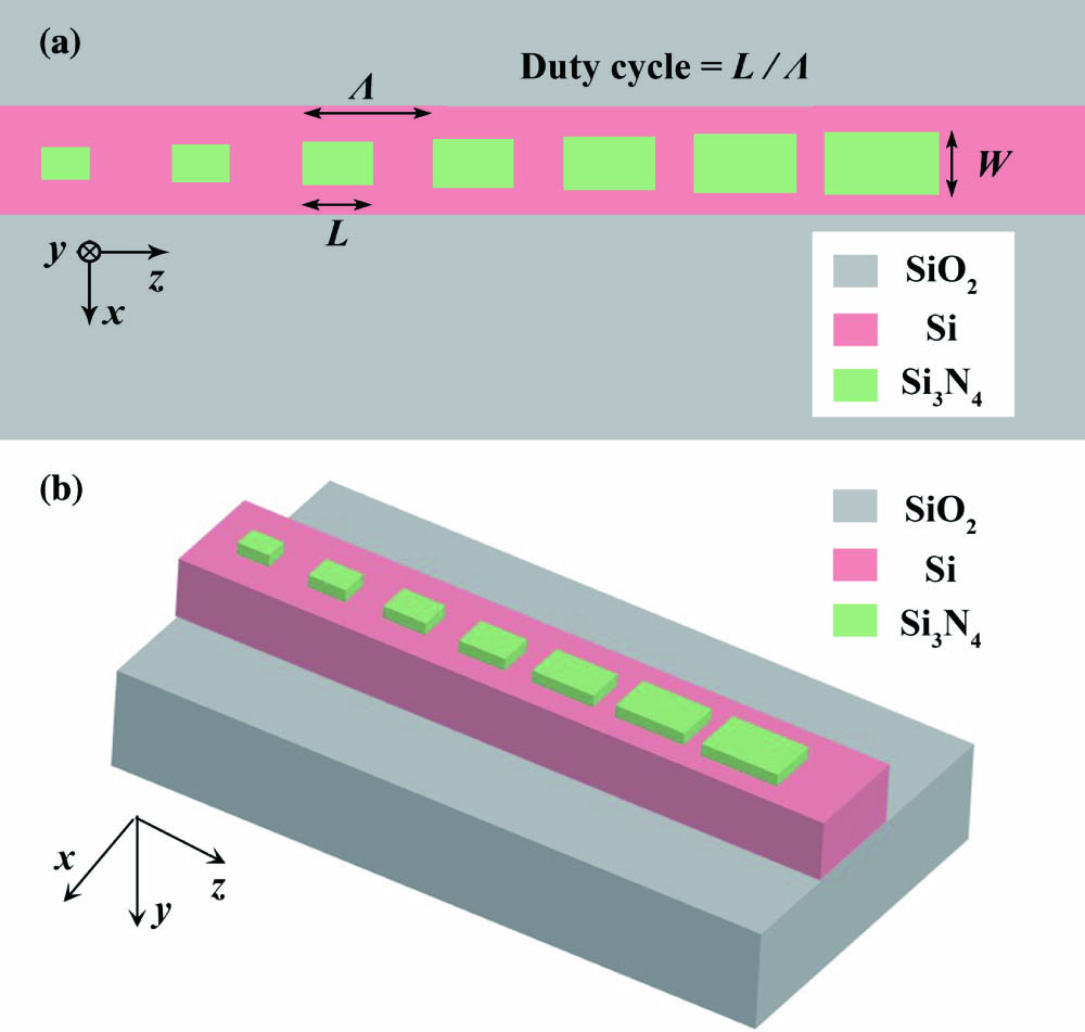
Shown schematically in Fig. 1, the customized grating is designed on a Si-on-insulator (SOI) platform. The Si waveguide has a height of 220 nm and a width of 500 nm. A overlayer with a height of 50 nm is deposited above the Si waveguide with cladding. The 2.247 mm grating contains 2500 grating periods totally with a period of 899.07 nm. The coupling between the guided mode and the radiation mode is constrained by the (quasi-)phase matching condition, and the radiation field consequently emerges at an angle of 30° (referenced to the grating facet normal). As a traveling wave with a fixed radiation angle, the radiation field has a planar phase front. In practice, 2500 independently parametrized overlayers undoubtedly increase the difficulty of actual fabrication and reduce the robustness of the device. An effective optimization strategy is proposed here by (1) grouping a series of 25 neighboring grating periods as an optimization group, where the widths and duty cycles of the overlayers are set to be identical; (2) constructing two fitting functions and , representing, respectively, the mapping relations from the group order S = 1–100 to the common widths and duty cycles of the overlayers in each group, to reduce the number of optimal variables. In particular, represents the percentage of the overlayer width to the Si core width. The fitting functions and can be expressed as
![]()
Figure 1.(a) Partial schematic diagram of our proposed Si3N4/Si grating with a varying duty cycle and width of the Si3N4 overlayer. (b) Our proposed grating’s 3D view without SiO2 cladding.
In our design, it is assumed that the guided mode is the mode, so . Then, substituting Eq. (5) into Eq. (4a), together with is , the attenuation of the guided mode can be expressed as
The attenuation of the mode per unit length along the direction can be given by
3. Result and Analysis
The optimized width and duty cycle distribution of the overlayers in each grating period are plotted in Fig. 2(a) as the solid black line and the solid red line, respectively. Assuming that the amplitude of the normalized fundamental guided mode is 1 (a.u.), the corresponding optimized emission profile at the wavelength of 1550 nm along the 2.247 mm grating length is plotted in Fig. 2(b). The solid black line represents the calculation result, agreeing well with a fitted Gaussian curve, having the expected value and variance , plotted with the solid red line. Their quantitative similarity can be expressed using the following cross-correlation coefficient formula, where and represent our optimized distribution of the emission profile and the corresponding fitted Gaussian profile, respectively:
![]()
Figure 2.(a) Optimized width and duty cycle distribution of the Si3N4 overlayer as a function of the grating period order. (b) The corresponding emission profile for our designed grating with a length of 2.247 mm at the wavelength of 1550 nm. (c) The major electric field distribution of the guided mode during the grating periods of 1145–1365. (d) The comparison of the calculated emission profile and the results simulated by FDTD in the same grating region.
At the wavelength of 1550 nm, the far-field beam profile for our proposed grating with the approximate Gaussian near-field emission intensity is shown in Fig. 3(a). The simulated FWHM beamwidth is as low as 0.026°, and the SSR is as high as 32.622 dB. Figure 3(b) illustrates the far-field intensity distribution for beam steering within the 1530–1570 nm wavelength range with a 5 nm step. A steering angle of 3.94° centered at 30° (working wavelength of 1550 nm) is achieved with approximately 0.1° per nanometer angular steering dispersion. Moreover, the far-field SSR for the 1530–1570 nm wavelength range is greater than 32 dB, suggesting that high-performance beam steering can be maintained during wavelength tuning.
![]()
Figure 3.(a) Far-field intensity distribution for our proposed grating at the 1550 nm wavelength. (b) Far-field intensity distribution for beam steering within 1530–1570 nm wavelength range with a 5 nm step.
In practice, deviations in fabricated dimensions of the overlayers from designed dimensions can lead to the radiation pattern change in our proposed grating antenna. To simulate the impact of fabrication errors as accurately as possible, we apply the Monte Carlo method to characterize the radiation fluctuations in the far field, assuming that the fabrication errors of the width and length (that is duty cycle) of the overlayer satisfy the Gaussian random distribution with mean value . Table 1 presents the averaged far-field SSR with the standard deviation varying from 10 nm to 60 nm, and Fig. 4 shows the error maps at , 40 nm, 50 nm, and 60 nm, respectively. The results show that the grating antenna can still maintain good performance with reasonable fabrication errors, e.g., below 30 nm, which is a quite exaggerated error for any state-of-the-art CMOS photonics foundry. Hence, our design could hold considerable merit and value in developing practical large aperture solid-state phase arrays.
![]()
Figure 4.Error maps of our proposed grating when σ = 30–60 nm, respectively. The red line indicates the average intensity, and the gray area represents the standard deviation of the intensity error at each point.
| Monte-Carlo Model | ||
|---|---|---|
| μ | σ (nm) | Average SSR (dB) |
| 0 | 10 | 32.227 |
| 20 | 30.766 | |
| 30 | 29.110 | |
| 40 | 26.130 | |
| 50 | 17.707 | |
| 60 | 15.379 | |
Table 1. Effect of Changes in Si3N4 Overlayer Width and Length on the SSR of Our Proposed Grating
4. Conclusion
In conclusion, we have proposed a practical design of a overlayer assisted Si grating emitter with an approximate Gaussian emission profile over length, which has a narrow angular FWHM of 0.026° and a large far-field SSR of 32.622 dB. The theory clearly reveals the general way to design a grating with a special emission profile by using CMT and GA. Further analysis shows that our emitter can also function well with almost undeteriorated angular divergence and SSR performance for the wavelength range from 1530 nm to 1570 nm, while achieving a longitudinal steering angle of about 3.94°. Our theoretical analysis indicates that our design is robust to practical fabrication errors for the width and length of the overlayer. We believe that the high-performance solid-state lidar systems can benefit from our demonstrated device.
References
[1] C. V. Poulton, A. Yaacobi, D. B. Cole, M. J. Byrd, M. Raval, D. Vermeulen, M. R. Watts. Coherent solid-state LIDAR with silicon photonic optical phased arrays. Opt. Lett., 42, 4091(2017).
[2] C. V. Poulton, M. J. Byrd, P. Russo, E. Timurdogan, M. Khandaker, D. Vermeulen, M. R. Watts. Long-range LiDAR and free-space data communication with high-performance optical phased arrays. IEEE J. Sel. Top. Quantum Electron., 25, 7700108(2019).
[3] C. V. Poulton, M. J. Byrd, E. Timurdogan, P. Russo, D. Vermeulen, M. R. Watts. Optical phased arrays for integrated beam steering. IEEE 15th International Conference on Group IV Photonics (GFP)(2018).
[4] C.-S. Im, B. Bhandari, K.-P. Lee, S.-M. Kim, M.-C. Oh, S.-S. Lee. Silicon nitride optical phased array based on a grating antenna enabling wavelength-tuned beam steering. Opt. Express, 28, 3270(2020).
[5] T. Raj, F. H. Hashim, A. B. Huddin, M. F. Ibrahim, A. Hussain. A survey on LiDAR scanning mechanisms. Electronics, 9, 741(2020).
[6] P. F. McManamon, P. Banks, J. Beck, D. G. Fried, A. S. Huntington, E. A. Watson. Comparison of flash lidar detector options. Opt. Eng., 56, 031223(2017).
[7] D. N. Hutchison, J. Sun, J. K. Doylend, R. Kumar, J. Heck, W. Kim, C. T. Phare, A. Feshali, H. Rong. High-resolution aliasing-free optical beam steering. Optica, 3, 887(2016).
[8] D. Kwong, A. Hosseini, J. Covey, Y. Zhang, X. Xu, H. Subbaraman, R. T. Chen. On-chip silicon optical phased array for two-dimensional beam steering. Opt. Lett., 39, 941(2014).
[9] S. A. Miller, Y.-C. Chang, C. T. Phare, M. C. Shin, M. Zadka, S. P. Roberts, B. Stern, X. Ji, A. Mohanty, O. A. Jimenez Gordillo, U. D. Dave, M. Lipson. Large-scale optical phased array using a low-power multi-pass silicon photonic platform. Optica, 7, 3(2020).
[10] J. Sun, E. Timurdogan, A. Yaacobi, E. S. Hosseini, M. R. Watts. Large-scale nanophotonic phased array. Nature, 493, 195(2013).
[11] L. Wang, Z. Chen, H. Wang, A. Liu, P. Wang, T. Lin, X. Liu, H. Lv. Design of a low-crosstalk half-wavelength pitch nano-structured silicon waveguide array. Opt. Lett., 44, 3266(2019).
[12] S. Jahani, S. Kim, J. Atkinson, J. C. Wirth, F. Kalhor, A. Al Noman, W. D. Newman, P. Shekhar, K. Han, V. Van, R. G. Decorby, L. Chrostowski, M. Qi, Z. Jacob. Controlling evanescent waves using silicon photonic all-dielectric metamaterials for dense integration. Nat. Commun., 9, 1893(2018).
[13] S. Jahani, Z. Jacob. Transparent subdiffraction optics: nanoscale light confinement without metal. Optica, 1, 96(2014).
[14] D. Kwong, A. Hosseini, J. Covey, X. Xu, Y. Zhang, S. Chakravarty, R. T. Chen. Corrugated waveguide-based optical phased array with crosstalk suppression. IEEE Photon. Technol. Lett., 26, 991(2014).
[15] B. Shen, R. Polson, R. Menon. Increasing the density of passive photonic-integrated circuits via nanophotonic cloaking. Nat. Commun., 7, 13126(2016).
[16] L. Zhang, Y. Li, Y. Hou, Y. Wang, M. Tao, B. Chen, Q. Na, Y. Li, Z. Zhi, X. Liu, X. Li, F. Gao, X. Luo, G.-Q. Lo, J. Song. Investigation and demonstration of a high-power handling and large-range steering optical phased array chip. Opt. Express, 29, 29755(2021).
[17] W. Xie, T. Komljenovic, J. Huang, M. Tran, M. Davenport, A. Torres, P. Pintus, J. Bowers. Heterogeneous silicon photonics sensing for autonomous cars [Invited]. Opt. Express, 27, 3642(2019).
[18] J. C. Hulme, J. K. Doylend, M. J. R. Heck, J. D. Peters, M. L. Davenport, J. T. Bovington, L. A. Coldren, J. E. Bowers. Fully integrated hybrid silicon two dimensional beam scanner. Opt. Express, 23, 5861(2015).
[19] M. Zadka, Y.-C. Chang, A. Mohanty, C. T. Phare, S. P. Roberts, M. Lipson. On-chip platform for a phased array with minimal beam divergence and wide field-of-view. Opt. Express, 26, 2528(2018).
[20] M. Raval, C. V. Poulton, M. R. Watts. Unidirectional waveguide grating antennas for nanophotonic phased arrays. Conference on Lasers and Electro-Optics (CLEO)(2017).
[21] B. Chen, Y. Li, L. Zhang, Y. Li, X. Liu, M. Tao, Y. Hou, H. Tang, Z. Zhi, F. Gao, X. Luo, G. Lo, J. Song. Unidirectional large-scale waveguide grating with uniform radiation for optical phased array. Opt. Express, 29, 20995(2021).
[22] S. Katoch, S. S. Chauhan, V. Kumar. A review on genetic algorithm: past, present, and future. Multimed. Tools Appl., 80, 8091(2021).
[23] Y. Song, F. Wang, X. Chen. An improved genetic algorithm for numerical function optimization. Appl. Intell., 49, 1880(2019).
[24] A. Arabali, M. Ghofrani, M. Etezadi-Amoli, M. S. Fadali, Y. Baghzouz. Genetic-algorithm-based optimization approach for energy management. IEEE Trans. Power Deliv., 28, 162(2013).
[25] D. Marcuse. Theory of Dielectric Optical Waveguides(1991).
[26] A. W. Snyder, R. A. Sammut. Radiation modes of optical waveguides. Electron. Lett., 15, 4(1979).
[27] C. G. Poulton, C. Koos, M. Fujii, A. Pfrang, T. Schimmel, J. Leuthold, W. Freude. Radiation modes and roughness loss in high index-contrast waveguides. IEEE J. Sel. Top. Quantum Electron., 12, 1306(2006).
[28] L. Ma, J. Li, Z. Liu, Y. Zhang, N. Zhang, S. Zheng, C. Lu. Intelligent algorithms: new avenues for designing nanophotonic devices [Invited]. Chin. Opt. Lett., 19, 011301(2021).

Set citation alerts for the article
Please enter your email address
© Copyright 2018-2021 | Chinese Laser Press. All Rights Reserved 沪ICP备15018463号-20