• Journal of Semiconductors
  • Vol. 42, Issue 1, 014103 (2021)
Ye Tao1、3, Xuhong Li1, Zhongqiang Wang1, Gang Li2, Haiyang Xu1, Xiaoning Zhao1, Ya Lin1, and Yichun Liu1
Author Affiliations
  • 1Key Laboratory for UV Light-Emitting Materials and Technology (Northeast Normal University), Ministry of Education, Changchun 130024, China
  • 2Hefei Institutes of Physical Science, Chinese Academy of Sciences, Hefei 230031, China
  • 3School of Science, Changchun University of Science and Technology, Changchun 130022, China
  • show less
    DOI: 10.1088/1674-4926/42/1/014103 Cite this Article
    Ye Tao, Xuhong Li, Zhongqiang Wang, Gang Li, Haiyang Xu, Xiaoning Zhao, Ya Lin, Yichun Liu. Neutron irradiation-induced effects on the reliability performance of electrochemical metallization memory devices[J]. Journal of Semiconductors, 2021, 42(1): 014103 Copy Citation Text show less

    Abstract

    In this work, electrochemical metallization memory (ECM) devices with an Ag/AgInSbTe (AIST)/amorphous carbon (a-C)/Pt structure were irradiated with 14 MeV neutrons. The switching reliability performance before and after neutron irradiation was compared and analyzed in detail. The results show that the irradiated memory cells functioned properly, and the initial resistance, the resistance at the low-resistance state (LRS), the RESET voltage and the data retention performance showed little degradation even when the total neutron fluence was as high as 2.5 × 10¹¹ n/cm2. Other switching characteristics such as the forming voltage, the resistance at the high-resistance state (HRS), and the SET voltage were also studied, all of which merely showed a slight parameter drift. Irradiation-induced Ag ions doping of the a-C layer is proposed to explain the damaging effects of neutron irradiation. The excellent hard characteristics of these Ag/AIST/a-C/Pt-based ECM devices suggest potential beneficial applications in the aerospace and nuclear industries.

    1. Introduction

    Stringent specifications for next-generation non-volatile memory devices have been imposed to overcome the ultimate limits of device physics and concomitant manufacturing technologies of conventional Si-based electronics[1-5]. One promising type of memory device employs electrochemical metallization memory (ECM), which has recently captured wide attention for its high storage density, fast programming speed, and ultra-low power consumption[6-12]. However, in extreme environmental conditions such as those encountered in applications for the aerospace industry and nuclear industry, such devices need to be strongly reliable when subjected to cosmic rays and nuclear irradiation[13]. Because of their neutral charge, neutrons–an abundant constituent of cosmic rays and nuclear radiation-possess very strong penetrability. During impact, neutrons collide with the atomic nuclei of materials with damaging consequences and thereby threaten their integrity and ultimately the device structure[14]. Therefore, thoroughly investigating the effects of neutron irradiation on the resistive switching reliability of ECM devices is quite necessary.

    Previous work on the characteristics of irradiation-hardened resistive switching memory devices is mostly based on gamma-ray radiation[15-18]. The work demonstrated that the ECM devices have a high tolerance to ionizing irradiation, even under total-ionizing-dose exposures exceeding several Mrad. However, for valence-change memory, the high-resistance state (HRS) is more easily affected by exposure effects, especially when the scale of the cell is relatively large[19]. The various reports highlighted the significance of material selection and device configuration concerning resistive switching memory once applied in irradiation-based systems. However, there is little work discussing the effects of neutron irradiation on the resistive switching characteristics of ECM devices. Taggart and colleagues reported that with increasing neutron fluence the Ag/GeSe-based CBRAM cells became irrecoverably locked into their final resistance state[20]. They attributed the malfunctioning of memory cells to displacement damage effects, which create significant material changes in the electrolyte layer, greatly inhibiting the mobility of Ag+ cations[20]. Indeed, Ag could dissolve into the chalcogenide once the Ag/chalcogenide interface is irradiated[21], resulting in a change in resistance of the memory cells. The primary cause that deteriorates the reliability of resistive memory still needs to be investigated.

    Our previous work had systematically evaluated the performance of Ag/AgInSbTe (AIST)/amorphous carbon (a-C)/Pt-based ECM devices. These devices show excellent resistive switching uniformity and good cycling endurance[22]. In this work, we further explore this highly reliable memory device to study the effects of neutron irradiation on its switching reliability. The device performance before and after neutron irradiation was compared and analyzed in detail. The irradiated devices function properly, without notable degradation, in regard to the SET/RESET voltages, endurance, and retention characteristics, whereas the HRS resistance was significantly impacted after irradiation. Furthermore, an Ag ion diffusion model is proposed to explain the neutron irradiation effects.

    2. Experimental section

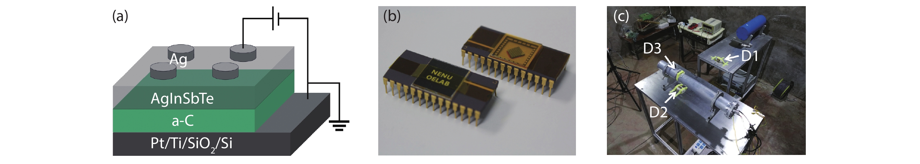
    Various ECM devices, each with an Ag/AIST/a-C/Pt structure [Fig. 1(a)] were fabricated. The depositions of the a-C layer and the AIST layer were done by RF magnetron sputtering of pure graphite and AIST (1 : 1 : 1 : 1) targets at room temperature. The thicknesses of the a-C and AIST layers were 20 and 15 nm, respectively. Finally, the top electrode metal Ag (50 nm) was thermally evaporated and patterned using a shadow mask with a diameter of 200 µm. In addition, these fabricated devices were mounted and wire bonded into ceramic dual in-line packages [see Fig. 1(b)]. The neutron irradiation experiments were conducted at the Institute of Radiation Technology of Northeast Normal University. For guaranteeing the working lifetime of our penning ion source neutron tube, the yield of the neutron tube was adjusted to ~ 5 × 10⁸ n/s. To achieve a series of different neutron fluences [see Fig. 1(c)], three packaged Ag/AIST/a-C/Pt devices were fastened in three different positions. These packaged memories devices were continuously irradiated for seven hours. Through simulation calculations, the total neutron fluences of the devices, here labeled D1, D2, and D3, were estimated at approximately 2.5 × 10⁹, 2.5 × 10¹⁰, and 2.5 × 10¹¹ n/cm2, respectively. A reference device, labeled D0, that was not irradiated by neutrons was used in comparisons with results. Then, these irradiated ECM devices were tested using a Keithley 2636A source meter. The current flow from the top to the bottom electrode is defined as the positive direction.

    (Color online) (a) Schematic diagrams of Ag/AIST/a-C/Pt ECM device. (b) Photograph of packaged Ag/AIST/a-C/Pt ECM devices. (c) Three devices were fastened in different positions to be exposed to different neutron fluences.

    Figure 1.(Color online) (a) Schematic diagrams of Ag/AIST/a-C/Pt ECM device. (b) Photograph of packaged Ag/AIST/a-C/Pt ECM devices. (c) Three devices were fastened in different positions to be exposed to different neutron fluences.

    3. Results and discussion

    First, we measured the initial resistance (IR) for 15 randomly selected devices from the four packaged ECM devices, D0, D1, D2, and D3. We found that the IR of the ECM cells [Fig. 2(a)] had not changed significantly and remained in the range from 105 to 107 Ω. As the resistance of the Ag/AIST/a-C/Pt devices mainly depends on the conductivity of the a-C film, we therefore deduce that the characteristics had not changed and interior structure of the a-C materials had not been damaged after neutron irradiation. Our previous reports had shown that pristine Ag/AIST/a-C/Pt devices need a forming process. For the four device packages for this work, we collected the forming voltage of each tested cell [Fig. 2(b)]. Clearly, the forming voltage gradually decreases with increasing neutron fluence. The forming process for the ECM devices has three main stages: Ag oxidation, Ag ions migration, and Ag ions reduction. In general, Ag oxidation occurs readily at the interface of Ag and the chalcogenide because its activation energy is low[23]. Furthermore, Dandamudi and colleagues demonstrated that once irradiated the Ag atoms spontaneously diffuse into the chalcogenide[21]. Therefore, we speculate that when the ECM devices are irradiated, many Ag atoms of the top electrode are oxidized and diffuse into the AIST layer, and even into the a-C layer, which explains why the forming voltage decreases.

    (Color online) (a) Initial resistance and (b) forming voltage of the four types of packaged ECM devices, D0, D1, D2, and D3, respectively.

    Figure 2.(Color online) (a) Initial resistance and (b) forming voltage of the four types of packaged ECM devices, D0, D1, D2, and D3, respectively.

    From the I–V curves taken from the four different ECM devices (Fig. 3), we see that our devices still operate normally even after being irradiated with a total neutron fluence of 2.5 × 10¹¹ n/cm2. To prevent the tested cells from hardening, a compliance current of 0.5 mA was subsequently applied during the SET process. To observe the evolutionary trend of the resistive switching memory clearly, we measured the values of the characteristic parameters from 50 normal cycles for D0, D1, D2, and D3. The HRS resistance, for instance, decreases gradually from ~ 4 × 10⁴ to ~ 6 × 10³ Ω with increasing total neutron fluence [Fig. 4(a)], whereas the low-resistance-state (LRS) resistance remains almost unchanged. Furthermore, the SET/RESET voltages [Fig. 4(b)] show either no really obvious variation or the number of subjects is too small to yield reliable results for reference.

    Typical I–V characteristics of D0, D1, D2 and D3.

    Figure 3.Typical I–V characteristics of D0, D1, D2 and D3.

    (Color online) (a) HRS and LRS variations and (b) SET and RESET voltage variations of the ECM devices D0, D1, D2, and D3.

    Figure 4.(Color online) (a) HRS and LRS variations and (b) SET and RESET voltage variations of the ECM devices D0, D1, D2, and D3.

    To reveal the variations in the resistive switching parameters, we randomly chose 15 cells from each ECM device package to perform a comparative analysis. The cumulative spread of HRS/LRS values [Fig. 5(a)] show that the median value of the HRS resistance indeed decreases along with increasing total neutron fluence; this behavior is consistent with the conclusion from the cycle variations [Fig. 4(a)]. In addition, the cumulative probability of SET/RESET voltages [Fig. 5(b)] show that the median value of the SET voltage increases with total neutron fluence. Although the irradiated ECM devices functioned properly, the values of the HRS resistance and the SET voltage had however both changed, suggesting that neutron irradiation may have had an impact on the material properties of the ECM devices. Knowing that the neutron beam penetrability is very strong, we write the attenuation process as[24]

    (Color online) (a) Device-to-device variation of LRS/HRS resistances and (b) SET and RESET voltages. Data was obtained for 15 randomly selected cells.

    Figure 5.(Color online) (a) Device-to-device variation of LRS/HRS resistances and (b) SET and RESET voltages. Data was obtained for 15 randomly selected cells.

     (1)

    where I0 and Iout denote the incident and transmitted beams, κ the attenuation coefficient of the material, and d the thickness of the material in the transmitted direction. With κ of the Ag top electrode being as much as 4.04, d is merely 50 nm. Thus, very few neutrons are absorbed or scattered by the top electrode during irradiation (< 0.01 %), implying that the AIST layer and the a-C layer are also irradiated with almost the same neutron fluence. The neutrons generated from our penning ion source neutron tube are almost fast neutrons (14 MeV), which on impact with atomic nuclei of the irradiated material undergo inelastic collision. According to previous reports, once irradiated, the Ag atoms spontaneously diffuse into a chalcogenide to form Ag ions[21], which directly augment the Ag ion concentration in the AIST layer. Therefore, it is highly possible that the Ag ions continue to migrate into the a-C layer through inelastic collisions. Thus, the a-C film close to the AIST layer will be doped with Ag ions [Fig. 6(b)].

    (Color online) Schematic diagrams of (a) the pristine ECM device, (b) the device after neutron irradiation, (c) the SET process, and (d) the RESET process.

    Figure 6.(Color online) Schematic diagrams of (a) the pristine ECM device, (b) the device after neutron irradiation, (c) the SET process, and (d) the RESET process.

    Figs. 6(b)(d) illustrate a possible mechanism that underscore the effects of neutron irradiation on resistive switching in the ECM memory devices. During the SET process [Fig. 6(c)], the redox reactions of the Ag atoms take place and induce Ag-ion migrations into the a-C layer, which then are reduced to Ag atoms on the surface of the bottom Pt electrode. With the continuous accumulation of Ag atoms, an Ag conductive filament is formed. The LRS resistance mainly depends on the characteristics of this filament rather than the insulating material (a-C layer). Therefore, the LRS resistance of each ECM device remains unchanged after neutron irradiation [Fig. 5(a)]. During the RESET process, the Ag atoms of the filament are oxidized and migrate back to the top electrode. In general, the filament ruptures at the narrowest point or at a location with maximum temperature[25-27]. Of interest is the low thermal conductivity of the AIST film, which results in low Joule heat diffusion at the AIST/a-C interface[28]. Therefore, the Ag conductive filament can rupture in the area close to the AIST/a-C interface [Fig. 6(d)], forming a tunneling gap between the filament and the AIST layer.

    From previous reports, the material characteristics of the gap determine the HRS resistance[29-31]. As mentioned above, the a-C film near the AIST/a-C interface is doped with Ag ions during neutron irradiation. A larger total neutron fluence results in a migration of more Ag ions. Hence, the dosage concentration of Ag ions in the a-C film increases with total neutron fluence as does the HRS resistance, which explains the results of Figs. 4(a) and 5(a). In addition, the SET voltage gradually increases with neutron fluence [Fig. 5(b)], the possible reason being that Ag ion scattering increases when they migrate into the a-C layer. Hence, a stronger electric field is needed to drive the migration of Ag ions, thereby resulting in a higher SET voltage[32-34].

    From the discussion above, we can see that the Ag/AIST/a-C/Pt ECM devices operate normally even during neutron beam irradiation. Aside from the resistive switching parameters, retention performance is another critical reliability issue. From the retention characteristics of both HRS and LRS for the four ECM device packages, D0–D3 (Fig. 7), the resistance values exhibit neither failure nor obvious degradation over 104 s, despite slight fluctuations in their resistance states, showing good potential retention characteristics of non-volatile storage.

    (Color online) Retention performance of the HRS and LRS of the four ECM device packages, D0, D1, D2, and D3.

    Figure 7.(Color online) Retention performance of the HRS and LRS of the four ECM device packages, D0, D1, D2, and D3.

    4. Conclusion

    The 14 MeV neutron irradiation effects on the resistive switching reliability of Ag/AIST/a-C/Pt-based ECM devices were investigated. We tested initial resistance, forming voltage, DC I–V curves, HRS/LRS resistance, SET/RESET voltage, and retention performance before and after neutron irradiation at various total fluences. A slight parameter drift was observed in the forming voltage, the HRS resistance, and the SET voltage, mainly through Ag ion injection into the a-C film near the AIST/a-C interface. Our ECM devices still functioned properly, demonstrating furthermore a robust tolerance to neutron irradiation and great promise in applications in both aerospace and nuclear industries.

    Acknowledgements

    This work was supported by the National Natural Science Foundation of China (Nos. 11974072, 52072065, 51732003, 51872043, 51902048, 61774031, 61574031, 62004016 and U19A2091), the NSFC for Distinguished Young Scholars (No. 52025022), the 111 Project (No. B13013), the fund from Ministry Education (No. 6141A02033414), the fund from Ministry of Science and Technology of China (Nos. 2018YFE0118300, 2019YFB2205100), the fund from Education Department of Jilin Province (No. JJKH20200734KJ), Open Foundation of Key Laboratory for UV-Emitting Materials and Technology of Ministry of Education, Northeast Normal University (No. 135130013), and the Innovative Research Funds of Changchun University of Science and Technology (No. XJJLG201907).

    References

    [1] et alCompact modeling of complementary switching in oxide-based ReRAM devices. IEEE Trans Electron Devices, 66, 1268(2019).

    [2] Nanoionics-based resistive switching memories. Nat Mater, 6, 833(2007).

    [3] et alProgrammable polymer thin film and non-volatile memory device. Nat Mater, 3, 918(2004).

    [4] et alFerroelastic switching for nanoscale non-volatile magnetoelectric devices. Nat Mater, 9, 309(2010).

    [5] Phase-change materials for non-volatile photonic applications. Nat Photonics, 11, 465(2017).

    [6] et alUniform multilevel switching of graphene oxide-based RRAM achieved by embedding with gold nanoparticles for image pattern recognition. Appl Phys Lett, 116, 163503(2020).

    [7] et alMoisture-powered memristor with interfacial oxygen migration for power-free reading of multiple memory states. Nano Energy, 71, 104628(2020).

    [8] et alPhotoassisted electroforming method for reliable low-power organic-inorganic perovskite memristors. Adv Funct Mater, 30, 1910151(2020).

    [9] et alToward a generalized Bienenstock-Cooper-Munro rule for spatiotemporal learning via triplet-STDP in memristive devices. Nat Commun, 11, 1(2020).

    [10] et alMemristors with organic-inorganic halide perovskites. InfoMat, 1, 183(2019).

    [11] et alSynaptic learning and memory functions achieved using oxygen ion migration/diffusion in an amorphous InGaZnO memristor. Adv Funct Mater, 22, 2759(2012).

    [12] et alImproved resistive switching reliability by using dual-layer nanoporous carbon structure. Appl Phys Lett, 111, 183504(2017).

    [13] et alLong-term and transient time variation of cosmic ray fluxes detected in Argentina by CARPET cosmic ray detector. J Atmos Sol-Terr Phy, 73, 1410(2011).

    [14] et alUnexpectedly large charge radii of neutron-rich calcium isotopes. Nat Phys, 12, 594(2016).

    [15] et alA study of gamma-ray exposure of Cu-SiO2 programmable metallization cells. IEEE Trans Nucl Sci, 62, 2404(2015).

    [16] et alTotal ionizing dose tolerance of Ag-Ge40S60 based programmable metallization cells. IEEE Trans Nucl Sci, 61, 1726(2014).

    [17] et alEffects of cobalt-60 gamma-rays on Ge-Se chalcogenide glasses and Ag/Ge-Se test structures. IEEE Trans Nucl Sci, 59, 3093(2012).

    [18] et alIonizing radiation effects on nonvolatile memory properties of programmable metallization cells. IEEE Trans Nucl Sci, 61, 2985(2014).

    [19] et alTotal ionizing dose (TID) effects on TaOx-based resistance change memory. IEEE Trans Electron Devices, 58, 2800(2011).

    [20]

    [21] et alFlexible sensors based on radiation-induced diffusion of Ag in chalcogenide glass. IEEE Trans Nucl Sci, 61, 3432(2014).

    [22] et alImproved uniformity and endurance through suppression of filament overgrowth in electrochemical metallization memory with AgInSbTe buffer layer. IEEE J Electron Devices, 6, 714(2018).

    [23] Electron self-trapping in Ge2Se3 and its role in Ag and Sn incorporation. Mater Res Soc Symp Proc, 1431(2012).

    [24] et alAn effective gamma white spots removal method for CCD-based neutron images denoising. Fusion Eng Des, 150, 11375(2020).

    [25] et alImproved switching reliability achieved in HfOx based RRAM with mountain-like surface-graphited carbon layer. Appl Surf Sci, 440, 107(2018).

    [26] Nano-graphite clusters regulation for reliability improvement of amorphous carbon-based resistive random access memory. Phys Status Solidi A, 216, 1900278(2019).

    [27] et alPerformance improvement of resistive switching memory achieved by enhancing local-electric-field near electromigrated Ag-nanoclusters. Nanoscale, 5, 4490(2013).

    [28] et alTemperature dependence of thermal properties of Ag8In14Sb55Te23 phase-change memory materials. Appl Phys A, 94, 627(2009).

    [29] Resistive switching memories based on metal oxides: mechanisms, reliability and scaling. Semicond Sci Tech, 31, 063002(2016).

    [30] et alBiodegradable natural pectin-based flexible multilevel resistive switching memory for transient electronics. Small, 15, 1803970(2019).

    [31] et alImprovement of resistive switching memory achieved by using arc-shaped bottom electrode. Appl Phys Express, 8, 014101(2014).

    [32] et alTotal ionizing dose (TID) effects of γ ray radiation on switching behaviors of Ag/AlOx/Pt RRAM device. Nanoscale Res Lett, 9, 452(2014).

    [33] et alHighly stable radiation-hardened resistive-switching memory. IEEE Electron Device Lett, 31, 1470(2010).

    [34] et alThree-dimensional observation of the conductive filament in nanoscaled resistive memory devices. Nano Lett, 14, 2401(2014).

    Ye Tao, Xuhong Li, Zhongqiang Wang, Gang Li, Haiyang Xu, Xiaoning Zhao, Ya Lin, Yichun Liu. Neutron irradiation-induced effects on the reliability performance of electrochemical metallization memory devices[J]. Journal of Semiconductors, 2021, 42(1): 014103
    Download Citation