
Zijiang Yang, Qiao Pan, Jiacheng Zhu, Weimin Shen. Fabrication of Silicon Echelle Grating by Ultraviolet Lithography Combined with Wet Etching[J]. Acta Optica Sinica, 2023, 43(13): 1305001
- Acta Optica Sinica
- Vol. 43, Issue 13, 1305001 (2023)
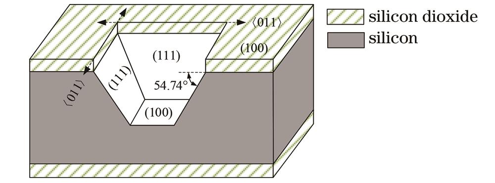
Fig. 1. Anisotropic etching of (100) monocrystalline silicon

Fig. 2. Schematics of echelle grating. (a) Traditional echelle grating; (b) silicon echelle grating
Fig. 3. Diffraction efficiency varying with platform duty ratio f at different working orders. (a) 47; (b) 41; (c) 36
Fig. 4. Tolerance analysis of grating platform duty ratio
Fig. 5. Fabrication process of echelle gratings. (a) Substrate pre-processing; (b) oxide layer growing; (c) photoresist spinning; (d) ultraviolet exposure and development; (e) oxygen plasma etching; (f) ICP etching; (g) wet etching; (h) high-reflecting film coating
Fig. 6. Grating after mask collapse under optical microscope
Fig. 7. Schematic of over-etching after reaching the self-stopping surface
Fig. 8. SEM photos of silicon echelle grating with or without crystal alignment. (a) Without crystal alignment; (b) with crystal alignment
Fig. 9. SEM photos of 42 lp/mm silicon echelle grating. (a) Magnification of 300×; (b) magnification of 1000×
Fig. 10. Grating photos after coating. (a) Top view; (b) dispersion diagram
Fig. 11. Schematic of diffraction efficiency testing device of echelle grating
Fig. 12. Measurement results of diffraction efficiency at corresponding blazed wavelength of working orders
Fig. 13. Test results of grating sidewall surface roughness
|
Table 1. Working parameters of grating
|
Table 2. Free spectral ranges corresponding to working diffraction orders of grating
|
Table 3. Parameters of grating groove
|
Table 4. Measurement results of grating


Set citation alerts for the article
Please enter your email address

© Copyright 2018-2021 | Chinese Laser Press. All Rights Reserved 沪ICP备15018463号-20