• Photonics Research
  • Vol. 11, Issue 5, 682 (2023)
Zihan Tao1、†, Yuansheng Tao1、†, Ming Jin1, Jun Qin2, Ruixuan Chen1, Bitao Shen1, Yichen Wu1, Haowen Shu1、6、*, Shaohua Yu1、3, and Xingjun Wang1、3、4、5、7、*
Author Affiliations
  • 1State Key Laboratory of Advanced Optical Communications System and Networks, School of Electronics, Peking University, Beijing 100871, China
  • 2Key Laboratory of Information and Communication Systems, Ministry of Information Industry, Beijing Information Science and Technology University, Beijing 100192, China
  • 3Peng Cheng Laboratory, Shenzhen 518055, China
  • 4Frontiers Science Center for Nano-optoelectronics, Peking University, Beijing 100871, China
  • 5Peking University Yangtze Delta Institute of Optoelectronics, Nantong 226010, China
  • 6e-mail: haowenshu@pku.edu.cn
  • 7e-mail: xjwang@pku.edu.cn
  • show less
    DOI: 10.1364/PRJ.476466 Cite this Article Set citation alerts
    Zihan Tao, Yuansheng Tao, Ming Jin, Jun Qin, Ruixuan Chen, Bitao Shen, Yichen Wu, Haowen Shu, Shaohua Yu, Xingjun Wang. Highly reconfigurable silicon integrated microwave photonic filter towards next-generation wireless communication[J]. Photonics Research, 2023, 11(5): 682 Copy Citation Text show less
    Operation principle and schematic of the IMPF. (a) The schematic of the chip layout. The add–drop port of the MRR is not shown because it was not used during the experiment. PM: phase modulator, ICSSA-CM: intensity-consistent single-stage-adjustable cascaded-microring, DR: dual ring, MRR: microring resonator, and PD: photodetector. (b) The operation principle of the realized multifunctional IMPF, including the bandpass filter and band-stop filter. (c) The operation schematic of the bandwidth and rejection ratio (RR) reconfigurability. (d) Optical microscope image of the whole IMPF.
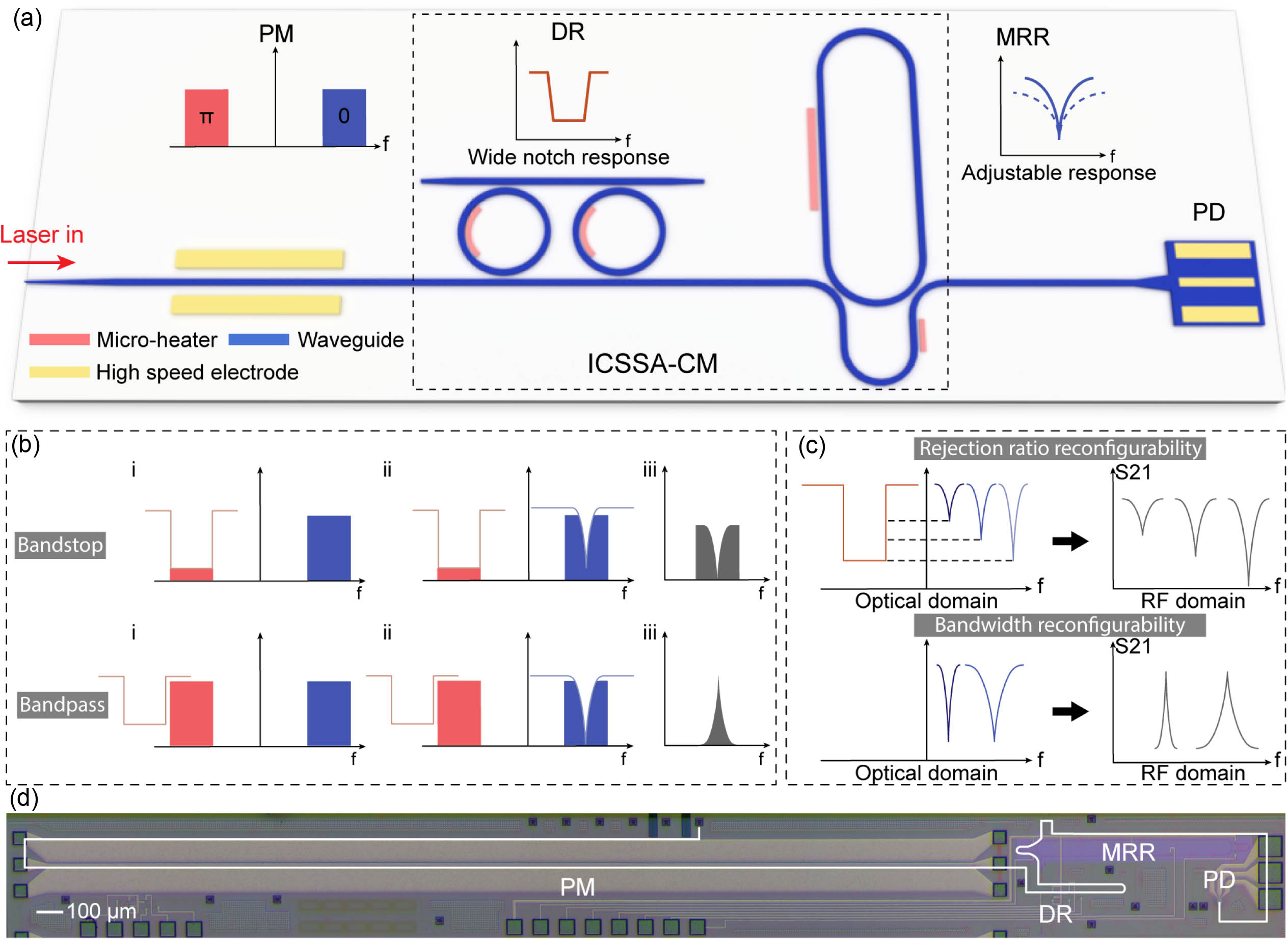
    Fig. 1. Operation principle and schematic of the IMPF. (a) The schematic of the chip layout. The add–drop port of the MRR is not shown because it was not used during the experiment. PM: phase modulator, ICSSA-CM: intensity-consistent single-stage-adjustable cascaded-microring, DR: dual ring, MRR: microring resonator, and PD: photodetector. (b) The operation principle of the realized multifunctional IMPF, including the bandpass filter and band-stop filter. (c) The operation schematic of the bandwidth and rejection ratio (RR) reconfigurability. (d) Optical microscope image of the whole IMPF.
    Measured results of the S21 response of the proposed IMPF. (a) and (c) Measured S21 response of the bandpass filter (BPF) with the central frequency tuned from 3 GHz to 24 GHz and the corresponding 3 dB bandwidths. (b) and (d) Measured S21 response of the band-stop filter (BSF) with the central frequency tuned from 5 GHz to 30 GHz and the corresponding 3 dB bandwidths. (e) The demonstration of the bandwidth reconfigurability via applying various voltages on the microheater on one arm of the AMZI. The bandwidth is tuned from 250 MHz to 2.07 GHz. (f) The demonstration of the RR reconfigurability. The RR is tuned from 12 dB to 50 dB. Additionally, the fluctuations of the bandwidth are within 170 MHz (from 360 MHz to 530 MHz). For better observation, each peak is intentionally detuned by a certain frequency when plotted. Other test results, such as dynamic range, can be found in Appendix C.
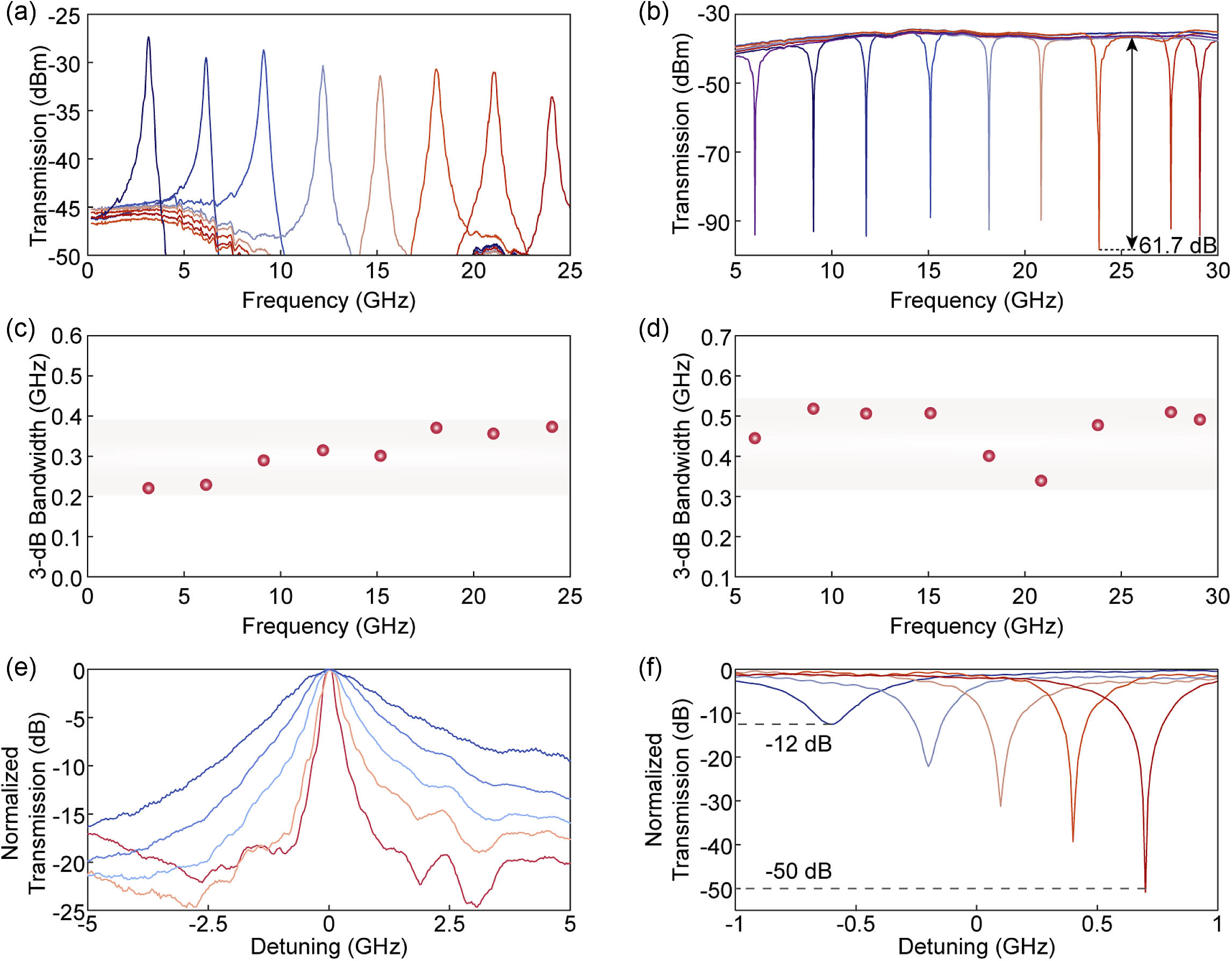
    Fig. 2. Measured results of the S21 response of the proposed IMPF. (a) and (c) Measured S21 response of the bandpass filter (BPF) with the central frequency tuned from 3 GHz to 24 GHz and the corresponding 3 dB bandwidths. (b) and (d) Measured S21 response of the band-stop filter (BSF) with the central frequency tuned from 5 GHz to 30 GHz and the corresponding 3 dB bandwidths. (e) The demonstration of the bandwidth reconfigurability via applying various voltages on the microheater on one arm of the AMZI. The bandwidth is tuned from 250 MHz to 2.07 GHz. (f) The demonstration of the RR reconfigurability. The RR is tuned from 12 dB to 50 dB. Additionally, the fluctuations of the bandwidth are within 170 MHz (from 360 MHz to 530 MHz). For better observation, each peak is intentionally detuned by a certain frequency when plotted. Other test results, such as dynamic range, can be found in Appendix C.
    Experimental demonstration of agile frequency channel selectivity in the microsecond-level response. (a) Diagram of the experimental setup. AWG: arbitrary waveform generator. DSO: digital storage oscilloscope. AFG: arbitrary function generator. (b) The time-frequency analysis of the filtered signals. The two channels are 6 GHz sine wave and 400 Mb/s QPSK signal modulated at 10 GHz carriers, respectively. (c) The power spectral density of two periods. Inset: the constellation of the 10 GHz channel (400 Mb/s QPSK signal). The down conversion process and coherent demodulation are carried out on an off-line desktop. The spurs in the spectrogram are induced by the DSO which is irrespective of experimental link.
    Fig. 3. Experimental demonstration of agile frequency channel selectivity in the microsecond-level response. (a) Diagram of the experimental setup. AWG: arbitrary waveform generator. DSO: digital storage oscilloscope. AFG: arbitrary function generator. (b) The time-frequency analysis of the filtered signals. The two channels are 6 GHz sine wave and 400 Mb/s QPSK signal modulated at 10 GHz carriers, respectively. (c) The power spectral density of two periods. Inset: the constellation of the 10 GHz channel (400 Mb/s QPSK signal). The down conversion process and coherent demodulation are carried out on an off-line desktop. The spurs in the spectrogram are induced by the DSO which is irrespective of experimental link.
    Experimental demonstration of the strong interference signal cancellation for the band-stop filter in wireless communication. (a) Diagram of the experimental setup and the operation principle of the strong image interference suppression for the notch filtering function. ESA: electronic spectrum analysis. LO: local oscillator. EA: electronic amplifier. (b) Photograph of the wireless experimental setup. (c) Spectra of the interference signal overlapping the filtered signal on the mixer IF port. (d) Constellation diagram with IMPF off and on.
    Fig. 4. Experimental demonstration of the strong interference signal cancellation for the band-stop filter in wireless communication. (a) Diagram of the experimental setup and the operation principle of the strong image interference suppression for the notch filtering function. ESA: electronic spectrum analysis. LO: local oscillator. EA: electronic amplifier. (b) Photograph of the wireless experimental setup. (c) Spectra of the interference signal overlapping the filtered signal on the mixer IF port. (d) Constellation diagram with IMPF off and on.
    Transmission of DR (left) and adjustable MRR (right).
    Fig. 5. Transmission of DR (left) and adjustable MRR (right).
    Measured transmission spectrum of the high-Q MRR.
    Fig. 6. Measured transmission spectrum of the high-Q MRR.
    Dynamic optical spectrum by changing the voltages on the microheaters.
    Fig. 7. Dynamic optical spectrum by changing the voltages on the microheaters.
    (a) Measured S21 responses of the PM. (b) Measured Vπ under different frequencies.
    Fig. 8. (a) Measured S21 responses of the PM. (b) Measured Vπ under different frequencies.
    (a) Measured S21 responses of the PD. (b) Measured responsivity of the PD.
    Fig. 9. (a) Measured S21 responses of the PD. (b) Measured responsivity of the PD.
    Experimental demonstration of the strong interference signal cancellation for the band-stop filter in the wired system. (a) Diagram of the experimental setup and the operation principle of the strong image interference suppression for the notch filtering function. MSG: microwave source generator. ESA: electronic spectrum analysis. LO: local oscillator. EA: electronic amplifier. (b) Spectra of the interference signal overlapping the filtered signal on the mixer IF port. (c) Constellation diagram with IMPF off and on.
    Fig. 10. Experimental demonstration of the strong interference signal cancellation for the band-stop filter in the wired system. (a) Diagram of the experimental setup and the operation principle of the strong image interference suppression for the notch filtering function. MSG: microwave source generator. ESA: electronic spectrum analysis. LO: local oscillator. EA: electronic amplifier. (b) Spectra of the interference signal overlapping the filtered signal on the mixer IF port. (c) Constellation diagram with IMPF off and on.
    Experimental demonstration of wireless communication for the bandpass filter. (a) Photograph of the wireless experimental setup. (b) Power spectral density of the signals. Blue: 10 GHz channel on. Red: 6 GHz channel on. (c) Constellation of the 10 GHz channel.
    Fig. 11. Experimental demonstration of wireless communication for the bandpass filter. (a) Photograph of the wireless experimental setup. (b) Power spectral density of the signals. Blue: 10 GHz channel on. Red: 6 GHz channel on. (c) Constellation of the 10 GHz channel.
    Measured output power of the IF fundamental tones and the IMD3 tones under different RF input powers for the BPF (left) and the BSF (right).
    Fig. 12. Measured output power of the IF fundamental tones and the IMD3 tones under different RF input powers for the BPF (left) and the BSF (right).
    Measured RF link loss (a) and noise (b) for the bandpass filter.
    Fig. 13. Measured RF link loss (a) and noise (b) for the bandpass filter.
    Test of the 1 dB compression point.
    Fig. 14. Test of the 1 dB compression point.
    YearIntegration LevelPlatformFunctionMax Frequency (GHz)Min Resolution (GHz)Bandwidth Tuning (GHz)Rejection Ratio Tuning (dB)RF Signal Transmission
    2020 [59]PassiveElectronicBPF or BSF62.4 (flatten)N/AN/AN/A
    2015 [43]PassiveSi3N4BPF, BSF, HT, etc.71.6Unfixed filter geometryUnfixed filter geometryN/A
    2017 [58]PassiveSOIBSF32.30.06N/A11.8–62.1N/A
    2017 [60]PassiveSi3N4BSF120.15N/AN/AN/A
    2019 [61]PassiveSi3N4BPF, BSF, and BR253.654.54–9.72N/AN/A
    2019 [62]LD, MD, and passiveInPBPF and BSF12.4Not shownN/AN/AN/A
    2021 [63]Passive and PDSOIBPF and BSF25Not shownN/AN/AN/A
    2021 [49]LD, MD, PD, and passiveInP + SOIBPF and BSF250.36N/AN/AN/A
    2022 [40]PassiveSi3N4+As2S3BSF200.5N/AN/A50 Mb/s QPSK
    2022 [46]LD, MD, and passiveAlGaAs + SOIBPF and BR211.971.97–2.42N/AN/A
    2022 [39]PassiveSOIBSF60.027N/AN/AN/A
    This workMD, PD, and passiveSOIBPF, BSF, BR, and RR300.220.25–212–502 Gb/s QPSK
    Table 1. Performance Comparison of State-of-the-Art IMPFsa
    Zihan Tao, Yuansheng Tao, Ming Jin, Jun Qin, Ruixuan Chen, Bitao Shen, Yichen Wu, Haowen Shu, Shaohua Yu, Xingjun Wang. Highly reconfigurable silicon integrated microwave photonic filter towards next-generation wireless communication[J]. Photonics Research, 2023, 11(5): 682
    Download Citation