1State Key Laboratory of Advanced Optical Communications System and Networks, School of Electronics, Peking University, Beijing 100871, China
2Key Laboratory of Information and Communication Systems, Ministry of Information Industry, Beijing Information Science and Technology University, Beijing 100192, China
3Peng Cheng Laboratory, Shenzhen 518055, China
4Frontiers Science Center for Nano-optoelectronics, Peking University, Beijing 100871, China
5Peking University Yangtze Delta Institute of Optoelectronics, Nantong 226010, China
Integrated microwave photonic filters (IMPFs) are capable of offering unparalleled performances in terms of superb spectral fineness, broadband, and more importantly, the reconfigurability, which encounter the trend of the next-generation wireless communication. However, to achieve high reconfigurability, previous works should adopt complicated system structures and modulation formats, which put great pressure on power consumption and controlment, and, therefore, impede the massive deployment of IMPF. Here, we propose a streamlined architecture for a wideband and highly reconfigurable IMPF on the silicon photonics platform. For various practical filter responses, to avoid complex auxiliary devices and bias drift problems, a phase-modulated flexible sideband cancellation method is employed based on the intensity-consistent single-stage-adjustable cascaded-microring (ICSSA-CM). The IMPF exhibits an operation band extending to millimeter-wave (), and other extraordinary performances including high spectral resolution of 220 MHz and large rejection ratio of 60 dB are obtained. Moreover, Gb/s-level RF wireless communications are demonstrated for the first time towards real-world scenarios. The proposed IMPF provides broadband flexible spectrum control capabilities, showing great potential in the next-generation wireless communication.
1. INTRODUCTION
The microwave filters are pivotal signal processing devices used to separate signals of interest from the background noise or to suppress the unwanted interference, and play an important role in the radio frequency (RF) front ends [1–4]. With the explosive growth of the wireless data rates in next-generation communication, the increment of signal density and band spreading to a higher frequency have led to increasingly complex electromagnetic environments filled with sorts of interferences [4–10]. As a result, the microwave filters are expected to be all-spectrum reconfigurable in the front ends for miscellaneous interferences suppression [11–15]. Meanwhile, for their massive deployment in wireless base stations [16,17], merits of low cost, low consumption, and light weight are also important considerations in which the state-of-the-art conventional electronic filters still show deficiency [18–20]. Solutions to meet all those requirements in RF signal processing remain elusive.
The integrated microwave photonic filters (IMPFs), widely known for the characteristics of ultrawide frequency tunability, are able to extend the operation range to the millimeter-wave and terahertz band [12,21–24]. With elaborate design and combination of photonic devices, versatile critical functions can be multiplexed in an individual system [25–32]. Meanwhile, the emerging photonic integration technique can effectively overcome the hurdles of size, reliability, and cost [33,34]. Up to now, a substantial quantity of solutions shows optimization in aspects, such as resolution [35–39], rejection ratio [40–42], reconfigurability [43–48], or footprint [49–51], respectively. Nonetheless, few have been well suited to achieve the synergy of all.
Previously, great efforts have been devoted to realizing such versatility. The programmable photonic processors either in the form of photonic mesh grid or tapped-delay-line structure, are considered to be highly reconfigurable [43,45–48]. However, large-scale arrays with repeating units are usually required in both cases for considerable performances, which leads to non-negligible optical loss and complicated collaborative controlling. Also, some photonic functional components utilized in these systems, such as long-time delay lines and large dispersion elements in a compact and integrated form, are still long-standing problems to be overcome. All above problems induce limitations in some key performances of an IMPF, in terms of spectral resolution and tuning range. On the other hand, some so-called application-specific IMPF circuits [35,49,52] by utilizing complicated modulation format and ultrafine optical filter [high- microring resonators (MRRs) or stimulated Brillouin scattering], are not sufficiently reconfigurable. Relying on the dual-parallel Mach–Zehnder modulator (MZM) [35,52] or a dual-drive MZM [49], the amplitude and phase of the sidebands can be controlled independently for designated filtering shape. However, this strategy strongly requires preprocessing of the RF signals with a series of bandwidth-limited electrical devices, which may obscure the promising of the IMPFs. Also, splitting the optical carrier into two or even four channels for electro-optical (EO) conversion induces the bias drift problem of the MZM, which will also hinder real-world communication applications. In other material platforms, such as thin-film lithium niobate, this could be particularly serious. Additionally, such optical filters, such as MRRs are prone to malfunction due to fabrication errors [53] so that they are not conducive to mass production. Therefore, balancing the versatility and performance is worth considering when designing an IMPF for practical applications.
Sign up for Photonics Research TOC. Get the latest issue of Photonics Research delivered right to you!Sign up now
In this paper, we demonstrate a wideband and highly reconfigurable IMPF based on a silicon-on-insulator (SOI) platform. The intensity-consistent single-stage-adjustable cascaded-microring (ICSSA-CM) architecture is proposed to carry out the phase-modulated flexible sideband cancellation method. Cooperating with the tunable amplitude, bandwidth, and coupling ratios of different microrings, the bandpass filter (BPF) and band-stop filter (BSF) with bandwidth and rejection ratio (RR) reconfigurability are simultaneously realized by shaping the phase-modulated spectrum. The IMPF shows unprecedented performances, including high spectral resolution (220 MHz), wide tuning range (up to 30 GHz), and high RR (around 60 dB, for BSF). Aiming to a simplified system operation, merely four microheaters are enough to switch among all functionalities, showing less power consumption and more compact size, which is extremely significant in massive deployments. Furthermore, the Gb/s-level QPSK wireless communication under image frequency interference and agile frequency channel selection are performed using the proposed IMPF, and it exhibits strong noise suppression ability and microsecond-level response, in practical scenarios. Such an IMPF will facilitate the further evolution of integrated microwave photonic systems towards ultrabroadband processing and real-time reconfigurability, which will substantially empower the next-generation wireless communication systems.
2. PRINCIPLE AND DESIGN
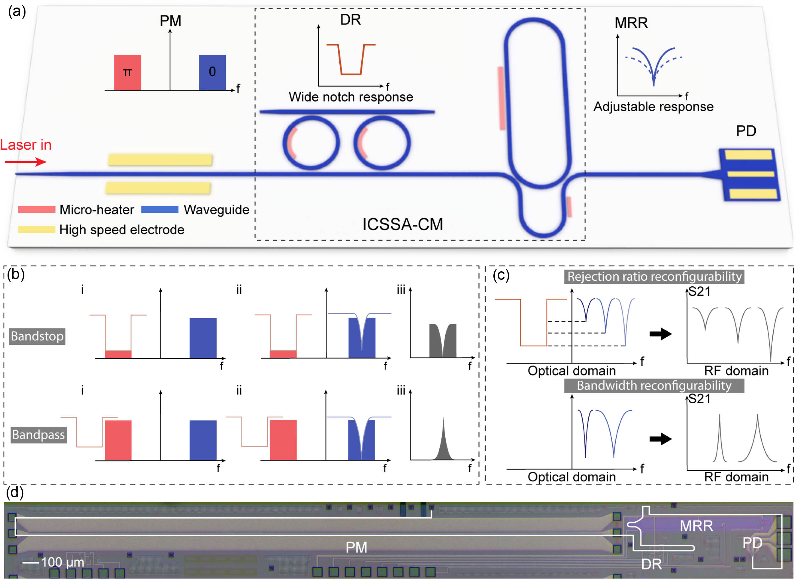
The architecture of the proposed IMPF is illustrated in Fig. 1(a). The layout consists of a PM, the ICSSA-CM, and a high-speed photodetector (PD). The PM enables large-bandwidth electrical-optical conversion and generates double sidebands with a -phase difference. A significant advantage of the PM is that no additional microheaters and feedback loops are required for bias stabilization control. The ICSSA-CM is formed of a wide notch-response dual-ring (DR) and a coupling-section-adjustable high- MRR. The wide notch response and the bandwidth-adjustable narrow notch response are, respectively, provided by the DR and the coupling-section-adjustable high- MRR. The modulated spectrum is tailored by these flexible responses and then directed to the PD to form the desired RF response.
Figure 1.Operation principle and schematic of the IMPF. (a) The schematic of the chip layout. The add–drop port of the MRR is not shown because it was not used during the experiment. PM: phase modulator, ICSSA-CM: intensity-consistent single-stage-adjustable cascaded-microring, DR: dual ring, MRR: microring resonator, and PD: photodetector. (b) The operation principle of the realized multifunctional IMPF, including the bandpass filter and band-stop filter. (c) The operation schematic of the bandwidth and rejection ratio (RR) reconfigurability. (d) Optical microscope image of the whole IMPF.
The working principle of the high reconfigurability is clearly shown in Figs. 1(b) and 1(c), and all types of filters can be formed by tuning the resonances of the DR and MRR with merely four microheaters. The upper sideband is tailored by the narrow notch response of MRR to select the desired frequency point in the RF domain. For BSF, the wide notch response of the DR is thermally tuned to suppress the lower sideband, and thus, an equivalent single-sideband modulation can be obtained. When the extinction ratios of the two responses are consistent, the amplitudes of sidebands at the desired frequency are equal, and complete cancellation is realized. For BPF, the resonance just needs to be moved away from the lower sideband and the PM to intensity modulation conversion (PM-IM) is performed [54,55]. Finally, the carrier and modified sidebands are mixed in the PD to form the corresponding RF filter. Moreover, the responses of the BSF and BPF can be further configured by simply adjusting the coupling state of the MRR. The flexible bandwidth of the BPF can be achieved by adjusting the coupling state of the MRR from undercoupling to overcoupling, in other words, the reduction of loaded- results in wider full width at half maximum (FWHM) of the MRR. Meanwhile, based on the sideband cancellation effect of the BSF, slightly different extinction ratios between two notch responses will result in a large difference in the RR of the RF response for handling different needs of interference rejection [56–58]. As shown above, the proposed method eliminates the effects of power imbalance and greatly simplifies on-chip operations.
Another potential benefit of the adjustable extinction ratio of the MRR is that the proposed IMPF is less sensitive to the fabrication errors. Since the fabrication errors can lead to spectral fluctuation of the two notch responses, the RR of the RF response becomes unpredictable. A coupling-section-adjustable design of the high- MRR can counteract the fluctuation to obtain the specified different extinction ratios between two responses. Additionally, such a design only needs to be applied on one MRR instead of all, which means reducing the number of microheaters and making the system lighter in weight, wieldy, and with lower power consumption. A detailed analysis can be found in Appendix A.
The proposed IMPF is fabricated on a complementary metal-oxide semiconductor (CMOS)-compatible 220 nm SOI platform in the CompoundTek foundry. The footprint is only , and the white line in Fig. 1(d) depicts the on-chip optical path. The PM has a length of 3.8 mm, and it is designed with traveling-wave electrodes for high-frequency RF signal input. The DR is designed with a 220 nm strip waveguide with two microheaters to control the position of resonance. The high- MRR utilizes an asymmetric MZ interferometer (AMZI) as a coupling region between the microring and the two bus waveguides for the adjustable coupling ratio. The rib waveguide with a 90 nm slab is implemented for -factor improvement. The width of the multimode waveguide is set as 2 μm to further improve the factor as well as to increase the free spectral range (FSR), and the designed length of the straight region is 600 μm. To avoid excitation of high-order modes, the multimode waveguide is tapered down to connect the single-mode bend of 450 nm with a radius of 30 μm. Besides, one microheater is applied on the straight waveguide of the microring, and the other is on the arm of AMZI on the bus waveguide. Spectral details of ICSSA-CM can be found in Appendix B. The PD connected to the through port of the MRR is designed as a vertical -doped-intrinsic--doped positive-intrinsic-negative (p-i-n) structure and is realized by the germanium (Ge) epitaxy growth technique for high-speed optical-electronic conversion.
3. EXPERIMENT RESULTS
A. Characterization on Basic Filtering Performances
An experiment was carried out to demonstrate the basic functionalities of the proposed IMPF. The vector network analyzer (VNA, Keysight N5247A) was used to measure the RF responses of the IMPF at different operation states. An external laser (EXFO, T100S-HP) was used to generate CW light with on-chip injection power of , which excludes the coupling loss of . The high-frequency microwave probes (Cascade Microtech, ACP40) were connected to the bond pads of on-chip PM and PD. Therefore, the VNA-generated RF signal with the power of 9 dBm could be sent to drive the PM. After processing by the IMPF, the recovered RF signal from the PD could be received. The power supply (Keysight, E36312A) offered bias voltage for the p-i-n junction via the bias tees (SHF, BT65D). Through the wire bonded to the print circuit board, four microheaters were controlled to tune the operating state of CMs.
As for the bandpass filtering function, the resonance of the DR was shifted far away from the optical carrier. As shown in Figs. 2(a) and 2(c), by tuning the microheater applied on the straight waveguide of the MRR, the central frequency of the passband can be continuously swept from 3 GHz to 24 GHz (around half of the FSR). Thanks to the high- factor, the minimum 3 dB bandwidth could reach 220 MHz, whereas the maximum RR reached 18.8 dB. To the best of our knowledge, this is the best performance among the reported BPFs with high integration levels (modulator, PD, and passive devices are all integrated on a monolithic chip).
Figure 2.Measured results of the S21 response of the proposed IMPF. (a) and (c) Measured S21 response of the bandpass filter (BPF) with the central frequency tuned from 3 GHz to 24 GHz and the corresponding 3 dB bandwidths. (b) and (d) Measured S21 response of the band-stop filter (BSF) with the central frequency tuned from 5 GHz to 30 GHz and the corresponding 3 dB bandwidths. (e) The demonstration of the bandwidth reconfigurability via applying various voltages on the microheater on one arm of the AMZI. The bandwidth is tuned from 250 MHz to 2.07 GHz. (f) The demonstration of the RR reconfigurability. The RR is tuned from 12 dB to 50 dB. Additionally, the fluctuations of the bandwidth are within 170 MHz (from 360 MHz to 530 MHz). For better observation, each peak is intentionally detuned by a certain frequency when plotted. Other test results, such as dynamic range, can be found in Appendix C.
With regard to the band-stop filtering function, the resonant frequency of the DR was shifted to eliminate the lower sideband generated by the PM. By precisely tuning the coupling state of the microring, complete cancellation between the upper and the lower sidebands could be satisfied. As shown in Figs. 2(b) and 2(d), the ultrahigh RR was obtained from 5 GHz to 30 GHz through continuous tuning of the MRR. The largest RR reaches up to 61.7 dB. In this mode, the frequency tuning range and the flatness of the passband are directly related to the notch response of the DR. More importantly, since the lower sideband is eliminated, the frequency tuning range can be expanded to one FSR of the MRR theoretically compared with the BPF.
For the validation of the bandwidth reconfigurability as shown in Fig. 2(e), the FWHM of the MRR was tuned by changing the coupling coefficient between the bus waveguide and the MRR. The results indicate that the proposed IMPF could achieve bandwidth adjustment from 250 MHz to 2.07 GHz. The RR reconfigurability was also proved by tuning the extinction ratio of the transmission of MRR [Fig. 2(f)]. The RR could be tuned from 12 dB to 50 dB. Theoretically, the controlling of these two functions is independent of the frequency tuning as the microheater was set on the bus waveguide, although the thermal cross talk might cause a slight shift in the resonance peak. This side effect could be compensated by reversely tuning the microheater on the straight waveguide of the MRR. Other test results, such as dynamic range, can be found in Appendix C.
B. Real-World Wireless Communications Based on the IMPF
In the real-world wireless RF signals transmission and receiving tasks, the RF receiver requires a BPF to separate the interest signals from the other channels. Rapid switching between different channels is also a rigid demand to meet the low latency [15]. Therefore, we performed an analog RF signal processing task to demonstrate the rapid channel selectivity. The experimental setup is depicted in Fig. 3(a). The operating state was set as a BPF, and the bandwidth was set to adapt the signal. The arbitrary waveform generator (AWG, Tektronix 70001B) was implemented to generate a 400 Mb/s QPSK signal modulated at 10 GHz, which was superimposed with a sinusoidal signal at 6 GHz to simulate two different channels at the same time. The generated signals were amplified via an electronic amplifier (EA) and then injected into the proposed IMPF. A square signal generated by an arbitrary function generator (AFG, RIGOL DG2102) was applied on the microheater on the straight waveguide of the MRR to make the central frequency hop between 6 GHz and 10 GHz. Figure 3(b) offers an intuitive visual representation of the time-frequency analysis of the rapid selecting response of the filtered signals received by the digital storage oscilloscope (DSO, Agilent DSA-X 96204Q) in the time window of 1 ms. The results demonstrated that an almost 20 dB RR can be achieved to select different frequency channels. Figure 3(c) shows the calculation of the power spectral density of the signals in different periods. To further prove the performance, an offline data process was carried out to simulate the down conversion of the QPSK signal, and the local oscillator (LO) frequency was set at 8 GHz to make the two channels alias together. The constellation of the processed signal shows that the symbols are separated clearly and the error vector magnitude (EVM) is 18.80%, which suggests that the 6 GHz channel was effectively suppressed. To demonstrate the capability of wireless communication for bandpass functionality, we also carried out the wireless task using the antenna. The details could be seen in Appendix E.
Figure 3.Experimental demonstration of agile frequency channel selectivity in the microsecond-level response. (a) Diagram of the experimental setup. AWG: arbitrary waveform generator. DSO: digital storage oscilloscope. AFG: arbitrary function generator. (b) The time-frequency analysis of the filtered signals. The two channels are 6 GHz sine wave and 400 Mb/s QPSK signal modulated at 10 GHz carriers, respectively. (c) The power spectral density of two periods. Inset: the constellation of the 10 GHz channel (400 Mb/s QPSK signal). The down conversion process and coherent demodulation are carried out on an off-line desktop. The spurs in the spectrogram are induced by the DSO which is irrespective of experimental link.
To demonstrate the strong interference suppression capability of the proposed IMPF, the other wireless communication experiment is conducted, and the setup is shown in Fig. 4(a). The proposed IMPF was set to the band-stop filtering function. The 2 Gb/s QPSK signal modulated at 10 GHz was generated by the AWG. A microwave source generator (MSG) provided a strong sinusoidal interference signal set at 11.8 GHz. The two signals were launched by two antennas whose operating frequency bands are 2–18 GHz and 10–28 GHz, respectively. The hybrid signals were received by another antenna and amplified by an EA. After being processed by the filter, the signals were amplified by the EA and down converted using the RF mixer. The frequency of the LO is 11 GHz. The schematic of the working principle shows that the interference would alias with the QPSK signals and deteriorate the EVM. After the mixer neither the hardware nor the software could eliminate such interference. In this case, a high RR notch RF filter to filter out the strong image interference before the mixer is critical for high-quality wireless communication.
Figure 4.Experimental demonstration of the strong interference signal cancellation for the band-stop filter in wireless communication. (a) Diagram of the experimental setup and the operation principle of the strong image interference suppression for the notch filtering function. ESA: electronic spectrum analysis. LO: local oscillator. EA: electronic amplifier. (b) Photograph of the wireless experimental setup. (c) Spectra of the interference signal overlapping the filtered signal on the mixer IF port. (d) Constellation diagram with IMPF off and on.
Figures 4(c) and 4(d) show the spectra of the filtered signals and the constellation after the mixer, respectively. The red line shown in Fig. 4(c) presents the superimposed interfering signal corresponding to Fig. 4(d) (left) where the filter is off, whereas the blue line presents the interference suppression signal corresponding to Fig. 4(d) (right). The proposed IMPF could suppress the intensity of the interference by nearly 20 dB, and the higher RR was masked by the power spectral density of QPSK. Due to the coupling angle mismatch of the jamming antenna, we reproduced the communication task under the wired system and coupled the two signals with an RF combiner to prove the capability of the high RR. The interference with the intensity of higher than 25 dB can be suppressed, and the details could be seen in Appendix D. The constellation (left) shows that the four points are aliased together, and the EVM is higher than 64% under the influence of the interfering signal. It is a normal situation that the center of the constellation is empty as the QPSK signal was disturbed by the constant amplitude and single-frequency tone. Although the constellation of the filter (right) shows that the four points are separated clearly, and the EVM is reduced to 24.48%. These results highlight the capability of the proposed IMPF as a multifunctional RF receiver in next-generation wireless communication systems.
4. DISCUSSION
Table 1 lists the key performances of state-of-the-art IMPFs and that in our paper. Our proposed IMPF is one of the few that realize a high integration level that the modulator, passive device, and PD are all integrated on a monolithic chip. The maximum frequency tuning range is up to 30 GHz, which is extended to the millimeter-wave band and is the broadest range without the dependence of commercial bulky modulator or PD. Benefiting from the delicate design of high- MRR, the minimum resolution of the proposed IMPF is nearly 220 MHz, outperforming other MRR-based IMPFs. We are the first to simultaneously achieve bandwidth and RR reconfigurability without any distortion of the filtering shape. These functionalities can be embedded in software-defined systems for various signals reception and unpredicted interference suppression, which is called cognitive radio [10,64]. Additionally, commercial devices, such as the optical bandpass filter, the dispersion element or delay line, are not necessary in our paper, which are essential components in other works. Note that even in some highly integrated works, the microwave devices, such as the 90° hybrid, are still needed [49], which are expensive and limited in phase and amplitude balance. The proposed IMPF here is capable to overcome this limitation where all key devices are integrated, and the RF signals can be directly injected and recovered. Our paper is also the first one to carry out the high-speed coherent signal (QPSK) up to the gigahertz rate, showing great potential for next-generation wireless communication in the high-speed rate. Above all, our paper achieves versatile functionalities and great performance with a compact footprint.
Not only that, the IMPF can achieve better performances by components optimization. First, to further improve the frequency tuning range, a larger FSR as well as a higher- silicon MRR can be utilized to fully cover the millimeter-wave band [31]. Additionally, the recently reported works about modulators and PDs on the SOI platform can support such a large bandwidth of OE/EO conversion [65–67]. Furthermore, based on the proposed architecture, the DR structure should be improved by cascading more microrings rather than dual rings, which may result in a wider notch response. Theoretically, the frequency range of the band-stop filter can be extended to one FSR if a wider notch response could cover this range. Meanwhile, this method could also make the edges of the wide notch response steeper so that the center frequency of the wide notch response could be closer to the carrier, extending tunable range towards far below 5 GHz. Second, the RR of the BPF is not high enough via PM-IM conversion. The reason is that the phase residual of the MRR reduces the suppression effect of the stop band. This phase response of the MRR will also affect the shape of the RF domain. The slopes of the rising and falling edges of the bandpass shape are slightly inconsistent, resulting in a relatively low RR and an asymmetry filtering shape, which can be further addressed by the two lasers method to compensate such a phase residual [68]. Third, to further improve the response time of the channel selectivity, the high- MRR should be improved to reduce the response time of the frequency shift of the resonant peak. One way is to add a p-i-n junction in the waveguide of the MRR, which can even realize gigahertz-level operation speed [69], whereas the p-i-n junction needs to be carefully designed to improve the response time with a slight influence on the factor. The second method is to specially design the microheater to use the parity-time symmetry breaking effect, and the response time can be reduced to μ [70]. As for the RF link performance, the insertion loss of the RF signal is mainly from the inefficient OE/EO conversion of the modulator and the PD, whereas the on-chip optical amplifier has been realized to solve it [71,72], and it is expected to be applied in system-on-chip applications in the future. Additionally, with the mature technology of the low noise microwave/millimeter-wave amplifier, the RF loss can be easily made up [73–75]. The BSF has an extra RF loss because the roll-off in the magnitude response of the DR is not steep enough that the optical carrier is partly filtered by that effect. A higher-order cascaded microring with a higher figure factor can easily cope with this problem [76]. As for the improvement of the dynamic range, the most important impediment to the dynamic range currently is the nonlinearity of the modulator, which results from the characteristic of the silicon-free-carrier dispersion modulation effect. That can be further improved when introducing the DC Kerr effect [77]. The combination of the plasma-dispersion effect and the DC Kerr effect could optimize the linearity of the silicon modulator, and the spurious free dynamic range (SFDR) greater than has been achieved. Moreover, by cascading more coupling-section-adjustable MRRs, multiple-independent-band filters can be obtained, which meets the need of 6G communication for multiband simultaneous operation and processing [15].
5. CONCLUSION
To summarize, we have demonstrated a wideband and highly reconfigurable IMPF with a streamlined structure on the SOI platform. Multiple filtering functions were implemented in a single chip with high performance. For the BPF, the tunable frequency was from 3 GHz to 24 GHz, and the minimum 3 dB bandwidth was 220 MHz. For the BSF, the tunable frequency was from 5 GHz to 30 GHz with a flat passband, and the RR was higher than 60 dB. The bandwidth reconfigurability and the RR reconfigurability were achieved from 250 MHz to 2.07 GHz and 12 dB to 50 dB, respectively. To validate the practicality of the proposed IMPF, the rapid channel selectivity experiment as well as the strong interference suppression experiment was carried out. Through the full cooperation between the on-chip devices, our proposed IMPF achieved the merits of high resolution, reconfigurability, ultrabroadband, fabrication insensitivity, light-weight, and low power consumption. Combining all these excellent performances would break the fundamental bottlenecks of 6G communication, and perform a critical step forward to the mass production and energy conservation of various microwave/millimeter wave applications.
APPENDIX A: PRINCIPLE OF HIGH RECONFIGURABILITY
As shown in Fig. 1(b), under small signal conditions and neglecting the high-order sidebands, the optical carrier after modulated by the PM can be described as where and denote the amplitude and the angular frequency of the optical carrier, denotes the PM index, denotes the half-wave voltage of the modulator, and denote the magnitude and angular frequency of the RF signal, and , , and are the 0th, 1st, and orders of Bessel function of the first kind. The PM spectrum is then tailored by the DR and high- MRR, which can be written as where denotes the response of the DR, and it takes 1 or 0 representing the BPF or BSF, respectively. is the complex transfer function of the high- MRR, and we assume that the resonance of the MRR is the fall in the upper sideband. According to the previous work [68], the phase residual of the MRR on the carrier and lower sideband cannot be ignored. Therefore, the beating photocurrent detected by the PD can be given as where and represent the phase residual induced by the MRR,
Note that the effect of the phase residual at the lower sideband will break the phase difference where the upper and lower sidebands are , resulting in incomplete out of phase cancellation in out-of-band for the RF response. That is the main factor limiting the RR of the BPF. For RR reconfigurability in the BSF, the response of the DR cannot completely cancel the lower sideband so that the cannot take 0 practically. Nevertheless, thanks to the adjustable coupling ratio for the MRR, the transfer function of the MRR can be changed to guarantee the condition, and the ultrahigh RR can be obtained. For different RRs, the formula can be summarized as
In theoretical calculations and a practical experiment, we found that a small change in the coupling ratio can achieve a relatively large RR adjustable. Therefore, the 3 dB bandwidth of the BSF can still maintain uniformity when tuning different RRs.
APPENDIX B: PERFORMANCE DETAILS OF ICSSA-CM
The DR offers a wide notch response in optical domain via weak electromagnetically induced transparency effect [25]. The bandwidth and extinction ratio can be flexibly tuned via thermally changing the relative position of the two resonances. Figure 5 (left) shows the normalized transmission in a wide notch band wider than 30 GHz in the optical domain. Although the proposed DR cannot achieve a higher extinction ratio, the results in the main text and the principle details in Appendix A indicate that the high RR can still be obtained in the RF domain if the extinction ratio of the adjustable MRR is consistent with the wide notch response. Figure 5 (right) shows the measured transmission spectrum of the resonance peaks from 1545 nm to 1560 nm at the through port. The magnitude envelope shows a wavelength-dependent periodic variation of the factor determined by the AMZI. The low magnitude peaks suggest that the factor is so high that the resolution of the optical spectrum analyzer (Yokogawa 6370C) is not precise enough to capture the full resonance peak shape.
Figure 5.Transmission of DR (left) and adjustable MRR (right).
The performances of the on-chip phase modulator in this IMPF were measured, through the on-chip power monitors composed of a 1:10 power splitter and a grating coupler. The optical insertion loss is around 5 dB at 1550 nm. We use the setup in Ref. [78] and extract the peak of the response to estimate the EO bandwidth of the PM. The 3 dB bandwidth is around 26 GHz. The data of the EO S21 response are collected by a VNA, and the processed data are shown in Fig. 8(a). The phase-shift efficiency () is also measured with the method in Ref. [79]. An MSG (Anritsu, MG3695A) was used to provide the single-tone RF signal, and an optical spectrometer (Yokogawa, 6370C) was used to record the power change in the carrier. The RF loss caused by the cable has been excluded. For each test, we take 10 sets of data and average them. The calculated results are shown in Fig. 8(b).
Figure 8.(a) Measured S21 responses of the PM. (b) Measured under different frequencies.
APPENDIX D: EXPERIMENT OF THE STRONG INTERFERENCE SIGNAL CANCELLATION IN A WIRED SYSTEM
We carried out the communication task in a wired system to achieve high coupling efficiency for the interference signal. The single-tone interference was set as 8.2 GHz, and the frequency of the LO was set as 9 GHz. The experimental setup is shown in Fig. 10(a). The proposed IMPF could suppress the intensity of the interference higher than 25 dB, and the higher RR was shaded by the power spectral density of the QPSK signal. The constellation [Fig. 10(c), left] shows that the four points are aliased together, and the EVM is higher than 66% under the influence of the interfering signal. While the constellation of the filter (right) shows that the four points are separated clearly, the EVM is reduced to 17.04%.
Figure 10.Experimental demonstration of the strong interference signal cancellation for the band-stop filter in the wired system. (a) Diagram of the experimental setup and the operation principle of the strong image interference suppression for the notch filtering function. MSG: microwave source generator. ESA: electronic spectrum analysis. LO: local oscillator. EA: electronic amplifier. (b) Spectra of the interference signal overlapping the filtered signal on the mixer IF port. (c) Constellation diagram with IMPF off and on.
APPENDIX E: EXPERIMENT OF THE WIRELESS COMMUNICATION FOR THE BANDPASS FILTER
We carried out the wireless communication task for the bandpass filter. The power supply (Keysight, E36312A) was used to change the voltage applied on the microheater on the high- MRR to switch the passband between two channels. The power spectral density of the two channels could be seen in Fig. 11(b). When the passband is tuned to the 10 GHz channel, the QPSK signal could be passed through, and we demodulated the constellation diagram at this time, as shown in Fig. 11(c). The EVM is 22.28% indicating that the bandpass filter has good performance in wireless communication.
Figure 11.Experimental demonstration of wireless communication for the bandpass filter. (a) Photograph of the wireless experimental setup. (b) Power spectral density of the signals. Blue: 10 GHz channel on. Red: 6 GHz channel on. (c) Constellation of the 10 GHz channel.
APPENDIX F: PERFORMANCE DETAILS FOR THE MICROWAVE LINK PARAMETER
In order to measure the SFDR for different types, a standard two-tone test was performed. Two RF tones at 6 GHz and 6.1 GHz were generated by two MSGs (Keysight E8257D and Anritsu MG3695A) and combined by an RF coupler. The two RF signals were directed to the PM via high-frequency microwave probes. The measured results are shown in Fig. 12. The left and right ones represent the BPF and BSF, respectively, and the two tones are located at the passband when testing different filter types. An ESA was used to measure the power of the fundamental components (FUND) and the third-order intermodulation components (IMD3, 5.9 GHz and 6.2 GHz). Under different RF input powers, the corresponding powers of the FUND and IMD3 were extracted and fitted with a measured noise floor of . The results show that the SFDR is and for the BPF and the BSF, respectively.
Figure 12.Measured output power of the IF fundamental tones and the IMD3 tones under different RF input powers for the BPF (left) and the BSF (right).
[19] E. J. Naglich, A. C. Guyette, D. Peroulis. High-Q intrinsically-switched quasi-absorptive tunable bandstop filter with electrically-short resonators. IEEE MTT-S International Microwave Symposium (IMS), 1-4(2014).
[56] W. Liu, W. Zhang, J. Yao. A bandstop microwave photonic delay-line filter with both tunable stop-band rejection ratio and tunable frequency. IEEE MTT-S International Microwave Symposium, 1-3(2015).
[57] B. A. Adoum, W. P. Wen. Investigation of band-stop to all pass reconfigurable filter. 4th International Conference on Intelligent and Advanced Systems (ICIAS), 1, 190-193(2012).
[65] C. Han, M. Jin, Y. Tao, B. Shen, H. Shu, X. Wang. Ultra-compact silicon modulator with 110 GHz bandwidth. Optical Fiber Communication Conference, Th4C-5(2022).
[73] Z. Chen, H. Gao, D. Leenaerts, D. Milosevic, P. Baltus. A 29–37 GHz BICMOS low-noise amplifier with 28.5 dB peak gain and 3.1–4.1 dB NF. IEEE Radio Frequency Integrated Circuits Symposium (RFIC), 288-291(2018).