• Journal of Semiconductors
  • Vol. 40, Issue 1, 012806 (2019)
Hui Hao1、2, Xiao Chen2, Zhengcheng Li2, Yang Shen2, Hu Wang2, Yanfei Zhao2, Rong Huang2, Tong Liu2, Jian Liang1, Yuxin An2, Qing Peng2, and Sunan Ding2
Author Affiliations
  • 1College of Materials Science and Engineering, Taiyuan University of Technology, Taiyuan 030024, China
  • 2Vacuum Interconnected Nanotech Workstation (Nano-X), Suzhou Institute of Nano-Tech and Nano-Bionics (SINANO), Chinese Academy of Sciences (CAS), Suzhou 215123, China
  • show less
    DOI: 10.1088/1674-4926/40/1/012806 Cite this Article
    Hui Hao, Xiao Chen, Zhengcheng Li, Yang Shen, Hu Wang, Yanfei Zhao, Rong Huang, Tong Liu, Jian Liang, Yuxin An, Qing Peng, Sunan Ding. Remote plasma-enhanced atomic layer deposition of gallium oxide thin films with NH3 plasma pretreatment[J]. Journal of Semiconductors, 2019, 40(1): 012806 Copy Citation Text show less
    (Color online) Schematic diagram of Ga2O3 thin film deposition process.
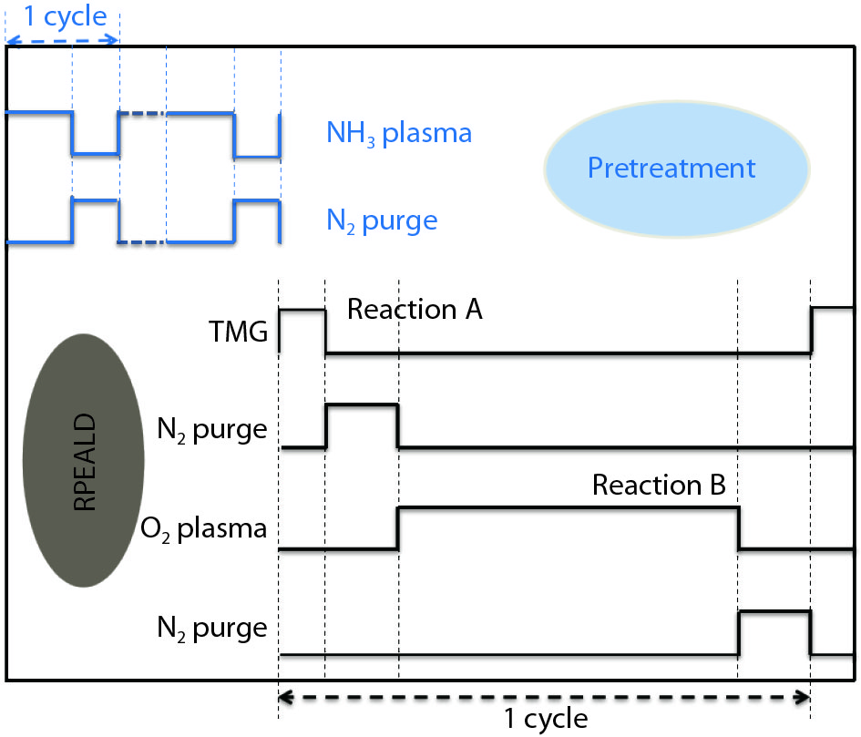
    Fig. 1. (Color online) Schematic diagram of Ga2O3 thin film deposition process.
    (Color online) (a) Growth rate of Ga2O3 films on Si as a function of O2 plasma flow duration at 250 °C. (b) Growth rate and O/Ga ratio of Ga2O3 films on Si as a function of temperature. (c) The Ga2O3 thin films thickness as a function of the number of RPEALD cycles. (d) A comparison of Ga2O3 deposition rates on Si between this work and the reported literatures.
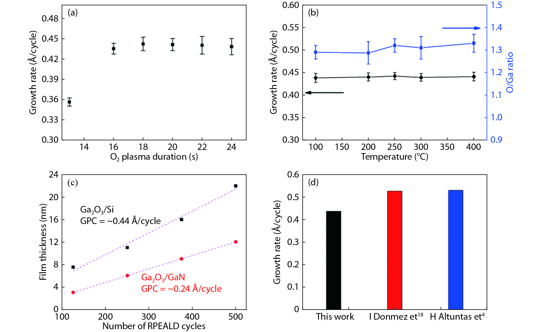
    Fig. 2. (Color online) (a) Growth rate of Ga2O3 films on Si as a function of O2 plasma flow duration at 250 °C. (b) Growth rate and O/Ga ratio of Ga2O3 films on Si as a function of temperature. (c) The Ga2O3 thin films thickness as a function of the number of RPEALD cycles. (d) A comparison of Ga2O3 deposition rates on Si between this work and the reported literatures.
    (Color online) Growth rate of Ga2O3 thin films as a function of NH3 plasma cycles.
    Fig. 3. (Color online) Growth rate of Ga2O3 thin films as a function of NH3 plasma cycles.
    (Color online) High resolution XPS spectra of (a) Ga3d core level and (b) O1s core level, in Ga2O3 films. The insets in (a) and (b) show the overlap of Ga3d and O1s peaks from the Ga oxide films deposited by different processes.
    Fig. 4. (Color online) High resolution XPS spectra of (a) Ga3d core level and (b) O1s core level, in Ga2O3 films. The insets in (a) and (b) show the overlap of Ga3d and O1s peaks from the Ga oxide films deposited by different processes.
    (Color online) AFM images of (a) Ga2O3 film deposited on Si without NH3 plasma treatment, (b) Ga2O3 film deposited on GaN without NH3 plasma treatment, (c) Ga2O3 film deposited on GaN with NH3 plasma treatment, and (d) a comparison of roughness between this work and previous reported literatures.
    Fig. 5. (Color online) AFM images of (a) Ga2O3 film deposited on Si without NH3 plasma treatment, (b) Ga2O3 film deposited on GaN without NH3 plasma treatment, (c) Ga2O3 film deposited on GaN with NH3 plasma treatment, and (d) a comparison of roughness between this work and previous reported literatures.
    (Color online) SIMS depth profiles of (a) Ga2O3/Si and (b) Ga2O3/GaN. The insets in (b) show 3D images of SIMS data reconstructions of Ga2O3/GaN.
    Fig. 6. (Color online) SIMS depth profiles of (a) Ga2O3/Si and (b) Ga2O3/GaN. The insets in (b) show 3D images of SIMS data reconstructions of Ga2O3/GaN.
    (Color online) High resolution XPS spectra of (a) Ga3d core level and (b) O1s core level on GaN surface.
    Fig. 7. (Color online) High resolution XPS spectra of (a) Ga3d core level and (b) O1s core level on GaN surface.
    (Color online) Ga3d core level spectra (a) w/o NH3 plasma and (b) with NH3 plasma, in Ga2O3 films.
    Fig. 8. (Color online) Ga3d core level spectra (a) w/o NH3 plasma and (b) with NH3 plasma, in Ga2O3 films.
    (Color online) the linear fitting of ln (1+R/R0) against 1/sinθ.
    Fig. 9. (Color online) the linear fitting of ln (1+R/R0) against 1/sinθ.
    (Color online) High resolution XPS spectra of Ga3d core level (a) w/o NH3 plasma and (b) with NH3 plasma, in Ga2O3 film.
    Fig. 10. (Color online) High resolution XPS spectra of Ga3d core level (a) w/o NH3 plasma and (b) with NH3 plasma, in Ga2O3 film.
    (Color online) HRTEM analysis of Ga2O3 films on GaN deposited by RPEALD. (a) Cross-sectional TEM image of a Ga2O3/GaN structure without NH3 plasma treatment. (a-1) Higher magnification views of the Ga2O3/GaN interface without NH3 plasma treatment. (a-2) FFT of Ga2O3 films deposited on GaN without NH3 plasma treatment. (b) Cross-sectional TEM image of a Ga2O3/GaN structure with NH3 plasma treatment. (b-1) Higher magnification views of the Ga2O3/GaN interface with NH3 plasma treatment. (b-2) FFT of Ga2O3 film deposited on GaN with NH3 plasma treatment.
    Fig. 11. (Color online) HRTEM analysis of Ga2O3 films on GaN deposited by RPEALD. (a) Cross-sectional TEM image of a Ga2O3/GaN structure without NH3 plasma treatment. (a-1) Higher magnification views of the Ga2O3/GaN interface without NH3 plasma treatment. (a-2) FFT of Ga2O3 films deposited on GaN without NH3 plasma treatment. (b) Cross-sectional TEM image of a Ga2O3/GaN structure with NH3 plasma treatment. (b-1) Higher magnification views of the Ga2O3/GaN interface with NH3 plasma treatment. (b-2) FFT of Ga2O3 film deposited on GaN with NH3 plasma treatment.
    ParameterPretreatment conditionDeposition condition
    Working pressure (hPa)1010
    Deposition temperature (°C)room temperature100, 200, 250, 300, 400
    Gas flow rate (sccm)150 (NH3 plasma), 40 (N2) 150 (TMG), 50 (O2 plasma), 50 (N2)
    Pulse/purge time (s)NH3 plasma (13), N2 (6) TMG (0.1), N2 (6), O2 plasma (13–20), N2 (6)
    Plasma generator power (W)2000 (NH3 plasma) 2800 (O2 plasma)
    Table 1. Deposition recipe for Ga2O3 thin films.
    Hui Hao, Xiao Chen, Zhengcheng Li, Yang Shen, Hu Wang, Yanfei Zhao, Rong Huang, Tong Liu, Jian Liang, Yuxin An, Qing Peng, Sunan Ding. Remote plasma-enhanced atomic layer deposition of gallium oxide thin films with NH3 plasma pretreatment[J]. Journal of Semiconductors, 2019, 40(1): 012806
    Download Citation