
Hui Hao, Xiao Chen, Zhengcheng Li, Yang Shen, Hu Wang, Yanfei Zhao, Rong Huang, Tong Liu, Jian Liang, Yuxin An, Qing Peng, Sunan Ding. Remote plasma-enhanced atomic layer deposition of gallium oxide thin films with NH3 plasma pretreatment[J]. Journal of Semiconductors, 2019, 40(1): 012806
- Journal of Semiconductors
- Vol. 40, Issue 1, 012806 (2019)
Abstract
1. Introduction
Oxide thin film is a kind of essential materials in semiconductor devices. Silicon dioxide, as a kind of dielectric material, has been playing a vitally important role in Si-based devices and the well-developed integrated circuit (IC) industry due to its excellent properties and the perfect matching with Si for interface passivation[
Plasma enhanced atomic layer deposition (PEALD) provides a number of advantages for preparing Ga2O3 thin film. It reduces the activation energies for the chemisorption of precursors at low-temperature growing films[
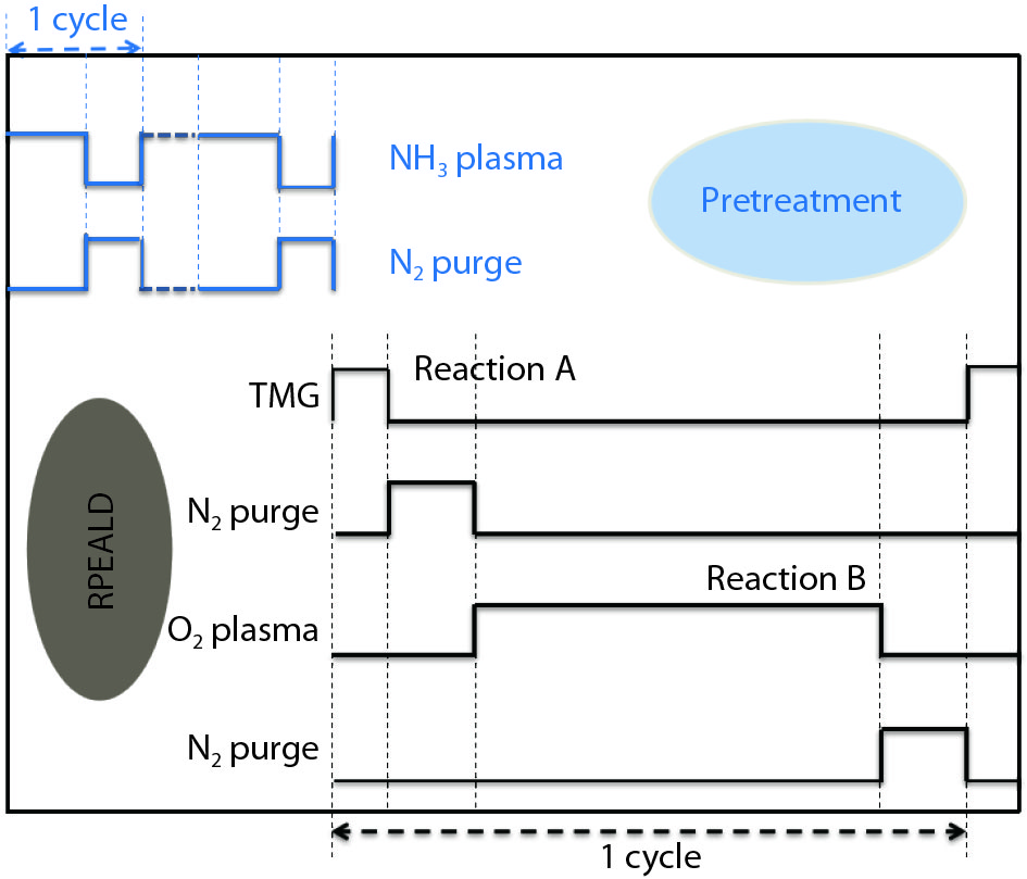
2. Experiment
Ga2O3 thin films were deposited by RPEALD (PICOSUN R-200 Advanced, Finland) using TMG (5N) as gallium source, ultra-pure O2 (6N) plasma as oxygen reactant with a base pressure of 10 hPa. N2 (5N) is used as carrier gas of TMG and purge gas of residues. Before the film deposited, 2-inch n-Si (100) wafers were first prepared with ultrasounds of acetone, isopropyl alcohol, and de-ionized (DI) water for 5 min each in sequence, then, cleaned in diluted HF solution (HF : H2O = 1 : 30) for removing native oxide, followed by DI water rinsing and pure N2 drying. GaN epi wafers (~1 × ~1 cm2) were cleaned similarly as Si substrates, except using NH4OH (25%–28%) instead of HF solution to remove intrinsic oxidation layer. After the ex-situ cleaning, Si wafers and GaN epi wafers were placed in the RPEALD chamber. The in-situ NH3 plasma pretreatment was conducted in the RPEALD reactor at room temperature (RF power 2000 W, 13 s of NH3 plasma and 6 s of N2 purge, 10–70 cycles of treatments). Then in each cycle, TMG, N2, O2, and N2 were introduced into the reactor in sequence, and the flow rates are 150, 50, 50, 50 sccm, respectively, as illustrated in Fig. 1. Ga2O3 films were deposited for 250 cycles on these substrates at a selected temperature from 100 to 400 °C. The detailed recipe is listed in Table 1, where one cycle consists of 0.1 s TMG (precursor temperature 0 °C) / 6 s N2 purge/13–24 s O2 plasma (RF power 2800 W)/6 s N2 purge.
![]()
Figure 1.(Color online) Schematic diagram of Ga2O3 thin film deposition process.
The thickness, crystal quality and surface morphology of Ga2O3 thin films were determined by ellipsometry (SE, M2000DI, J. A. Woollam), high resolution transmission electron microscope (HR-TEM, Tecnail G2 F20 S-Twin, FEI) and atomic force microscope (AFM, Dimension ICON, Burker). X-ray photoelectron spectroscopy (XPS, PHI 5000 Versa Probe II, ULVAC-PHI), together with time-of-flight secondary ion mass spectroscopy (TOF-SIMS 5, IONTOF), were employed to characterize the film chemical composition, bonding states and impurities from the surface to interface.
3. Results and discussion
To explore the growth parameters of Ga oxide, effects of TMG dose, O2 plasma duration, and temperature on the growth rate were studied. The TMG dose is represented by its pulse duration, which is found no effect on the deposition rate when it changes from 0.1 to 0.2 s, indicating that the shortest duration of 0.1 s is enough to reach a saturation. Fig. 2(a) shows the deposition rate of Ga oxide on Si as a function of O2 plasma flow duration, with fixed TMG dose of 0.1 s and growth temperature of 250 °C. The growth rate increases with O2 plasma duration and saturates when it exceeds 18 s. In order for the reaction to be sufficient, we chose 20 s as O2 plasma duration. As Fig. 2(b) shows, the deposition rate and chemical ratio of the films are almost independent to growth temperature in a wide range, similar to other reports[
![]()
Figure 2.(Color online) (a) Growth rate of Ga2O3 films on Si as a function of O2 plasma flow duration at 250 °C. (b) Growth rate and O/Ga ratio of Ga2O3 films on Si as a function of temperature. (c) The Ga2O3 thin films thickness as a function of the number of RPEALD cycles. (d) A comparison of Ga2O3 deposition rates on Si between this work and the reported literatures.
It has been reported[
![]()
Figure 3.(Color online) Growth rate of Ga2O3 thin films as a function of NH3 plasma cycles.
All Ga oxide films grown on Si and GaN, with and without NH3 pretreatment, were characterized by XPS to analyze their composition and chemical states. The O1s and Ga3d core levels were collected from the as-grown surfaces with an emission angle of 45º, and calibrated by C1s peak (assigned at 284.8 eV) to align the binding energies of all peaks. In Fig. 4, the Ga3d (a) and O1s (b) peaks of Ga oxide films deposited by different processes are overlapped and fitted by using CasaXPS software. For Ga3d, the peak with binding energy of ~20.5 eV is attributed to Ga–O bonding[
![]()
Figure 4.(Color online) High resolution XPS spectra of (a) Ga3d core level and (b) O1s core level, in Ga2O3 films. The insets in (a) and (b) show the overlap of Ga3d and O1s peaks from the Ga oxide films deposited by different processes.
One of the ALD technique advantages is high conformity and uniformity. The surface morphology of Ga2O3 thin films deposited on Si and GaN were characterized by AFM, as shown in Fig. 5. The surface of Ga2O3 film on Si is smoother than that of Ga2O3 on GaN, which shows clearly step flow as following the features of GaN epi wafer. The surface roughness of the two Ga2O3 thin films are 0.12 and 0.20 nm respectively. Comparing with the results reported by others[
![]()
Figure 5.(Color online) AFM images of (a) Ga2O3 film deposited on Si without NH3 plasma treatment, (b) Ga2O3 film deposited on GaN without NH3 plasma treatment, (c) Ga2O3 film deposited on GaN with NH3 plasma treatment, and (d) a comparison of roughness between this work and previous reported literatures.
Therefore, it is likely that the substrate surface condition was modified somehow by the plasma. We conducted TOF-SIMS depth profiling to check the interfaces of oxides and substrates (Si and GaN). As shown in Fig. 6, with 250 cycles deposition, the oxide film thicknesses are increased on pretreated Si substrate and GaN epi wafer respectively. Meanwhile, the counts of H− and OH− secondary ions are obviously increased at the interfaces after NH3 pretreatment. The 3D depth profile images of SIMS data reconstructions, as the inserts in Fig. 6(b), clearly represent the distribution of OH− on the oxide surfaces and at the oxide/substrate interfaces. To further confirm the difference in the density of OH− components, XPS was conducted on GaN epi wafer to investigate the GaN surfaces before and after NH3 treatment, as shown in Fig. 7. The Ga3d and O1s core level peaks are fitted into related components, according to published references[
![]()
Figure 6.(Color online) SIMS depth profiles of (a) Ga2O3/Si and (b) Ga2O3/GaN. The insets in (b) show 3D images of SIMS data reconstructions of Ga2O3/GaN.
![]()
Figure 7.(Color online) High resolution XPS spectra of (a) Ga3d core level and (b) O1s core level on GaN surface.
In order to further verify the effect of NH3 plasma on initial growth, we determined the thickness of very thin gallium oxides by using Angle-resolved XPS measurement. The Ga3d core-level spectra for the Ga2O3 film of 10 cycles growing obtained at different photoelectron collecting angle (θ) are shown in Fig. 8. Each Ga3d peak can be well fitted the peak of the Ga–N and Ga–O bonds. The thicknesses of the thin films are estimated to be 4.8 ± 0.1 Å for Ga2O3 film without NH3 plasma and 7.9 ± 0.4 Å for Ga2O3 film with NH3 plasma, based on Eq. (1) given as follows[
![]()
Figure 8.(Color online) Ga3d core level spectra (a) w/o NH3 plasma and (b) with NH3 plasma, in Ga2O3 films.
where R is the areal ratio of Ga–O component to Ga–N component under the Ga3d spectrum; R0 is related to the bulk material properties of Ga2O3 and GaN, it is calculated according to material densities, formula weights and inelastic mean free path (IMFP); d is thickness of the Ga2O3 film; λ0 is electron IMFP of Ga2O3 film. A plot of ln (1 + R/R0) against 1/sin θ is linear with a slope of d/λ0, from which the thickness d can be decided, as shown in Fig. 9. The deposition rate of Ga2O3 film of the first 10 cycles was increased after NH3 plasma treatment. It is noticed that the trend of growth rate change is consistent with the above result, which confirmed the initial growth are enhanced by increasing hydroxide radicals on the substrate surfaces, and NH3 pretreatment is an effective way to activate the surface bonding states.
![]()
Figure 9.(Color online) the linear fitting of ln (1+
To further confirm the mechanism of initial growth, we check the chemical states of Ga2O3 films deposited with different cycles. As shown in the Fig. 10, the Ga3d peaks shift to higher binding energy with more Ga2O3 deposited. For the same deposition cycles, the amount of the peak shift in Fig. 10(a) is about 0.11 eV smaller than that in Fig. 10(b), meaning thicker Ga2O3 films are formed on the surface with NH3 plasma pretreatment than that without the pretreatment. All the results prove that the NH3 plasma pretreatment enhanced the initial growth rate of Ga2O3 thin layer, because more active sites are generated on the substrate surfaces.
![]()
Figure 10.(Color online) High resolution XPS spectra of Ga3d core level (a) w/o NH3 plasma and (b) with NH3 plasma, in Ga2O3 film.
High resolution TEM is a powerful technique for atomic structure analysis of thin film and interface. The as-grown films deposited on GaN exhibit ordered arrangement of atoms in a certain level, as shown clearly in Figs. 11(a) and 11(b). The FFT (fast Fourier transform) patterns in Figs. 11(a-2) and 11(b-2) demonstrate the crystallization of low temperature (~250 °C) growth of Ga2O3 film with an interplanar distance of 4.63 Å, corresponding to (−201) face of β-Ga2O3[
![]()
Figure 11.(Color online) HRTEM analysis of Ga2O3 films on GaN deposited by RPEALD. (a) Cross-sectional TEM image of a Ga2O3/GaN structure without NH3 plasma treatment. (a-1) Higher magnification views of the Ga2O3/GaN interface without NH3 plasma treatment. (a-2) FFT of Ga2O3 films deposited on GaN without NH3 plasma treatment. (b) Cross-sectional TEM image of a Ga2O3/GaN structure with NH3 plasma treatment. (b-1) Higher magnification views of the Ga2O3/GaN interface with NH3 plasma treatment. (b-2) FFT of Ga2O3 film deposited on GaN with NH3 plasma treatment.
4. Conclusions
In summary, high quality Ga2O3 thin films were deposited by remote plasma-enhanced atomic layer deposition within a wide temperature window. With in-situ NH3 plasma pretreatment, the deposition rate of Ga2O3 is enhanced remarkably due to more hydroxyls generated on the substrate surface. This pretreatment has no effect on the stoichiometry and surface morphology of Ga2O3 films, indicating NH3 plasma only modify the surface states of substrate by enhancing reactive site density. Ga2O3 films grown on GaN wafer is crystallized even at 250 °C, with an epitaxial interface between Ga2O3 and GaN. Those results open a new way to reduce the interface states in GaN based devices by passivating GaN surfaces with epitaxial Ga2O3 thin films.
Acknowledgements
This work was supported jointly by the National Natural Science Foundation of China (Nos. 61674165, 61604167, 61574160, 61704183, 61404159, 11604366), the Natural Science Foundation of Jiangsu Province (Nos. BK20170432, BK20160397, BK20140394), the National Key R&D Program of China (No. 2016YFB0401803), and the Strategic Priority Research Program of the Chinese Academy of Science (No. XDA09020401). SE, AFM, and TEM characterizations were performed through the support at the Platform for Characterization &Test, Suzhou Institute of Nano-Tech and Nano-Bionics (SINANO), Chinese Academy of Sciences.
References
[1] S U Engelmann, R S Wise, L Meng et al. Facile fabrication of Si-based nanostructures. Proc SPIE, 10149, 1014910(2017).
[2] Y Hori, Z Yatabe, T Hashizume. Characterization of interface states in Al2O3/AlGaN/GaN structures for improved performance of high-electron-mobility transistors. J Appl Phys, 114, 244503(2013).
[3] F K Shan, G X Liu, W J Lee et al. Structural, electrical, and optical properties of transparent gallium oxide thin films grown by plasma-enhanced atomic layer deposition. J Appl Phys, 98, 023504(2005).
[4] H Altuntas, I Donmez, C Ozgit-Akgun et al. Electrical characteristics of β-Ga2O3 thin films grown by PEALD. J Alloys Compd, 593, 190(2014).
[5] A A Dakhel. Investigation of opto-dielectric properties of Ti-doped Ga2O3 thin films. Solid State Sci, 20, 54-58(2013).
[6] A Szyszka, L Lupina, G Lupina et al. Ultraviolet GaN photodetectors on Si via oxide buffer heterostructures with integrated short period oxide-based distributed Bragg reflectors and leakage suppressing metal–oxide–semiconductor contacts. J Appl Phys, 116, 083108(2014).
[7] H Y Shih, F C Chu, A Das et al. Atomic layer deposition of gallium oxide films as gate dielectrics in AlGaN/GaN metal–oxide–semiconductor high-electron-mobility transistors. Nanoscale Res Lett, 11, 235(2016).
[8] T Yamada, J Ito, R Asahara et al. Improved interface properties of GaN-based metal-oxide-semiconductor devices with thin Ga-oxide interlayers. Appl Phys Lett, 110, 261603(2017).
[9] G X Liu, F K Shan, J J Park et al. Electrical properties of Ga2O3-based dielectric thin films prepared by plasma enhanced atomic layer deposition (PEALD). J Electroceram, 17, 145(2006).
[10] F P Yu, S Ou, D S Wuu. Pulsed laser deposition of gallium oxide films for high performance solar-blind photodetectors. Opt Mater Express, 5, 1240(2015).
[11] M F Al-Kuhaili, S M A Durrani, E E Khawaja. Optical properties of gallium oxide films deposited by electron-beam evaporation. Appl Phys Lett, 83, 4533(2003).
[12] T Takeuchi, H Ishikawa, N Takeuchi et al. High resolution X-ray photoelectron spectroscopy of beta gallium oxide films deposited by ultra high vacuum radio frequency magnetron sputtering. Thin Solid Films, 516, 4593(2008).
[13] S Ghose, S Rahman, L Hong et al. Growth and characterization of β-Ga2O3 thin films by molecular beam epitaxy for deep-UV photodetectors. J Appl Phys, 122, 095302(2017).
[14] M Baldini, M Albrecht, A Fiedler et al. Semiconducting Sn-doped β-Ga2O3 homoepitaxial layers grown by metal organic vapour-phase epitaxy. J Mater Sci, 51, 3650(2015).
[15] K Sasaki, Q T Thieu, D Wakimoto et al. Depletion-mode vertical Ga2O3 trench MOSFETs fabricated using Ga2O3 homoepitaxial films grown by halide vapor phase epitaxy. Appl Phys Express, 10, 124201(2017).
[16] G A Battiston, R Gerbasi, M Porchia et al. Chemical vapour deposition and characterization of gallium oxide thin films. Thin Solid Films, 279, 115(1996).
[17] D J Comstock, J W Elam. Atomic layer deposition of Ga2O3 films using trimethylgallium and ozone. Chem Mater, 24, 4011(2012).
[18] I Donmez, C Ozgit-Akgun, N Biyikli. Low temperature deposition of Ga2O3 thin films using trimethylgallium and oxygen plasma. J Vac Sci Technol A, 31, 01A110(2013).
[19] D W Choi, K B Chung, J S Park. Low temperature Ga2O3 atomic layer deposition using gallium tri-isopropoxide and water. Thin Solid Films, 546, 31(2013).
[20] R K Ramachandran, J Dendooven, J Botterman et al. Plasma enhanced atomic layer deposition of Ga2O3 thin films. J Mater Chem A, 2, 19232(2014).
[21] R O'Donoghue, J Rechmann, M Aghaee et al. Low temperature growth of gallium oxide thin films via plasma enhanced atomic layer deposition. Dalton Trans, 46, 16551(2017).
[22] B Hoex, S B S Heil, E Langereis et al. Ultra low surface recombination of c-Si substrates passivated by plasma-assisted atomic layer deposited Al2O3. Appl Phys Lett, 89, 042112(2006).
[23] J M Park, S J Jang, L L Yusup et al. Plasma-enhanced atomic layer deposition of silicon nitride using a novel silylamine precursor. ACS Appl Mater Interfaces, 8, 20865(2016).
[24] H B Profijt, S E Potts, M C M van de Sanden et al. Plasma-assisted atomic layer deposition: basics, opportunities, and challenges. J Vac Sci Technol A, 29, 050801(2011).
[25] M Bose, D K Basa, D N Bose. Effect of ammonia plasma pretreatment on the plasma enhanced chemical vapor deposited silicon nitride films. Mater Lett, 48, 336(2001).
[26] J Yang, B S Eller, R J Nemanich. Surface band bending and band alignment of plasma enhanced atomic layer deposited dielectrics on Ga- and N-face gallium nitride. J Appl Phys, 116, 123702(2014).
[27] D Li, J Huang, D Yang. Enhanced electroluminescence of silicon-rich silicon nitride light-emitting devices by NH3 plasma and annealing treatment. Physica E, 41, 920(2009).
[28] I Krylov, A Gavrilov, D Ritter et al. Elimination of the weak inversion hump in Si3N4/InGaAs (001) gate stacks using an in situ NH3 pre-treatment. Appl Phys Lett, 99, 203504(2011).
[29] J M Park, S J Jang, S I Lee et al. Novel Cyclosilazane-type silicon precursor and two-step plasma for plasma-enhanced atomic layer deposition of silicon nitride. ACS Appl Mater Interfaces, 10, 9155(2018).
[30] B J Kim, Y C Kim, J J Lee. The effect of NH3 plasma pre-treatment on the adhesion property of (Ti1-
[31] E S Aydil. Real time in situ monitoring of surfaces during glow discharge processing: NH3 and H2 plasma passivation of GaAs. J Vac Sci Technol B, 13, 258(1995).
[32] M J Tadjer, M A Mastro, N A Mahadik et al. Structural, optical, and electrical characterization of monoclinic β-Ga2O3 grown by MOVPE on sapphire substrates. J Electron Mater, 45, 2031(2016).
[33] H S Oon, K Y Cheong. Recent development of gallium oxide thin film on GaN. Mater Sci Semicond Process, 16, 1217(2013).
[34] P Jaiswal, U Ul Muazzam, A S Pratiyush et al. Microwave irradiation-assisted deposition of Ga2O3 on III-nitrides for deep-UV opto-electronics. Appl Phys Lett, 112, 021105(2018).
[35] X Y Deng, C Weis, H Bluhm et al. Adsorption of water on Cu2O and Al2O3 thin films. J Phys Chem C, 112, 9668(2008).
[36]
[37] T L Duan, J S Pan, D S Ang. Investigation of surface band bending of Ga-face GaN by angle-resolved X-ray photoelectron spectroscopy. ECS J Solid State Sci Technol, 5, 514(2016).

Set citation alerts for the article
Please enter your email address
© Copyright 2018-2021 | Chinese Laser Press. All Rights Reserved 沪ICP备15018463号-20