• NUCLEAR TECHNIQUES
  • Vol. 45, Issue 10, 100401 (2022)
Zhi LIU1, Guodong GAO1、2, Junhui YUE1, Jianshe CAO1、2, Yaoyao DU1, Huizhou MA1, Jun HE1, Qiang YE1, Xuhui TANG1、2, Yukun LI1、2, Jing YANG1、2, and Shujun WEI1、2、*
Author Affiliations
  • 1Institute of High Energy Physics, Chinese Academy of Sciences, Beijing 100049, China
  • 2University of Chinese Academy of Sciences, Beijing 100049, China
  • show less
    DOI: 10.11889/j.0253-3219.2022.hjs.45.100401 Cite this Article
    Zhi LIU, Guodong GAO, Junhui YUE, Jianshe CAO, Yaoyao DU, Huizhou MA, Jun HE, Qiang YE, Xuhui TANG, Yukun LI, Jing YANG, Shujun WEI. Design and verification of data acquisition clock circuit based on dual-loop phase-locked loop[J]. NUCLEAR TECHNIQUES, 2022, 45(10): 100401 Copy Citation Text show less
    SNR of ADC when clock jitter is 1 ps, 2 ps and 5 ps
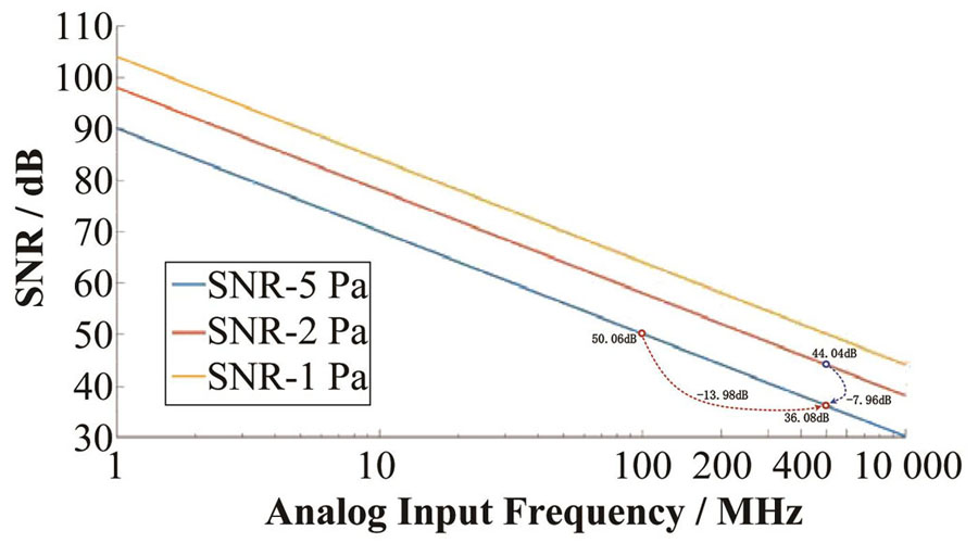
    Fig. 1. SNR of ADC when clock jitter is 1 ps, 2 ps and 5 ps
    The working principle of PLL
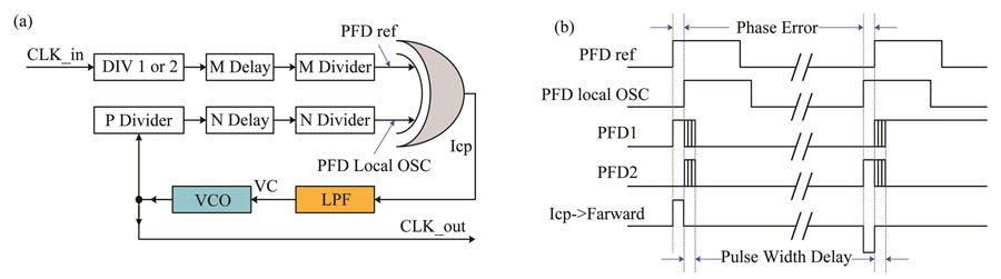
    Fig. 2. The working principle of PLL
    Simplified functional block diagram for LMK04610
    Fig. 3. Simplified functional block diagram for LMK04610
    Block diagram of dual-loop phase-locked loop system overall design
    Fig. 4. Block diagram of dual-loop phase-locked loop system overall design
    Diagrammatic drawing of power supply design
    Fig. 5. Diagrammatic drawing of power supply design
    Diagrammatic drawing of the configuration circuit
    Fig. 6. Diagrammatic drawing of the configuration circuit
    Equivalent circuit model of Balun (a), diagrammatic drawing of input/output (b)
    Fig. 7. Equivalent circuit model of Balun (a), diagrammatic drawing of input/output (b)
    Design of PLL1 LPF and its phase noise
    Fig. 8. Design of PLL1 LPF and its phase noise
    Test for jitter performance (a) The jitter of source clock, (b) The jitter of processed clock
    Fig. 9. Test for jitter performance (a) The jitter of source clock, (b) The jitter of processed clock
    SNR of ADC band-pass sampling data when the clock jitter is 1.8 ps
    Fig. 10. SNR of ADC band-pass sampling data when the clock jitter is 1.8 ps
    Zhi LIU, Guodong GAO, Junhui YUE, Jianshe CAO, Yaoyao DU, Huizhou MA, Jun HE, Qiang YE, Xuhui TANG, Yukun LI, Jing YANG, Shujun WEI. Design and verification of data acquisition clock circuit based on dual-loop phase-locked loop[J]. NUCLEAR TECHNIQUES, 2022, 45(10): 100401
    Download Citation