
Hongyue Hao, Donghai Wu, Yingqiang Xu, Guowei Wang, Dongwei Jiang, Zhichuan Niu. Research progress of high performance Sb-based superlattice mid-wave infrared photodetector (Invited)[J]. Infrared and Laser Engineering, 2022, 51(3): 20220106
- Infrared and Laser Engineering
- Vol. 51, Issue 3, 20220106 (2022)
![Summary of the most reported data of minority carrier lifetimes at 77 K for Ga-free T2 SL, InAs/GaSb T2 SL, HgCdTe/MCT, and other binary and ternary III–V material systems[9]](/richHtml/irla/2022/51/3/20220106/img_1.jpg)
Fig. 1. Summary of the most reported data of minority carrier lifetimes at 77 K for Ga-free T2 SL, InAs/GaSb T2 SL, HgCdTe/MCT, and other binary and ternary III–V material systems[9]
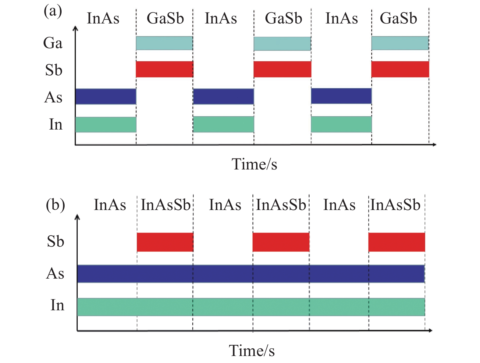
Fig. 2. Shutter sequences used in MBE growth of (a) InAs/GaSb type-II superlattice (T2 SLs) and (b) InAs/InAsSb T2 SLs
Fig. 3. (a) Band alignment of InAs/AlAs/InAsSb T2 SLs; (b) Shutter sequences used in InAs/InAsSb absorber growth; (c) Shutter sequences used in InAs/AlAs/InAsSb barrier growth; (d) The 0th diffraction peak and Sb component in InAs/AlAs/InAsSb SLs by varying the Sb/As flux ratio; (e) High-resolution X-ray diffraction (HRXRD) experimental (blue) and simulation (red) curve of the InAs/InAsSb SLs; (f) FWHM in HRXRD pattern of 5.6/2.2/5.6/7.5 mL InAs/AlAs/InAs/InAsSb SLs samples with different interfaces between InAs and AlAs layer[14]
Fig. 4. (a) Bright-field HRTEM images, (b) HRTEM images parallel to the growth direction, (c) Strain tensorεyy map of the 5.6/2.2/5.6/8 mL InAs/AlAs/InAs/InAsSb SLs [14]
Fig. 5. (a) Band alignment of the InAs/InAs0.45Sb0.55 absorber; (b) Band alignment of the AlAs0.45Sb0.55/InAs0.45Sb0.55 barrier layer; (c) Schematic diagram of the p+-B-n device energy band structure; (d) Curves of dark current density with bias of the p+-B-n photodetectors at different temperature; (e) Dark current density of the p+-B-n photodetector under -100 mV applied bias [17]
Fig. 6. (a) Au photocrystals photodiodes[18]; (b) Nano-tenna structures[19]; (c) Deposit Ge-grating structures[20]
Fig. 7. (a) Structure of InGaAsSb/AlGaAsSb photodiodes with photon-trap arrays; (b) SEM image off photon-trap arrays; (c) Design of photon-trap arrays;Response of the photodiodes with (red) and without (black) photon-trap arrays at (d) 400-1600 nm and (e) 1.5-3 μm; (f) Dark current density at different temperature [23]
Fig. 8. (a) Reflection, (b) responsibility at 400-800 nm, (c) 800 nm-2 μm, (d) 3-5 μm of the photon-trap array photodiodes[24]
Fig. 8. [in Chinese]
Fig. 9. Three different kinds of photon-trap arrays (Tetrahedron, pyramid, cylinder)
Fig. 10. Three dimensional views of the photon-traps of (a) hole prism PTs and (b) Quadrangular prism PTs; (c) Calculated reflectivity changes with an edge length of arrays, quadrangular (red) and hole (blue)[25]

Set citation alerts for the article
Please enter your email address
© Copyright 2018-2021 | Chinese Laser Press. All Rights Reserved 沪ICP备15018463号-20