• Laser & Optoelectronics Progress
  • Vol. 60, Issue 3, 0312003 (2023)
Jiamin Liu1, Hang Zhao1, Qizhe Wu1, Xianrui Feng1, Xiangyu Zhao1, Zhenyang Zhang1, Chumiao Zhang1, Tao Huang2、**, Jinlong Zhu1、3、*, and Shiyuan Liu1、3、***
Author Affiliations
  • 1State Key Laboratory of Digital Manufacturing Equipment and Technology, Huazhong University of Science and Technology, Wuhan 430074, Hubei, China
  • 2School of Mechanical Science & Engineering, Huazhong University of Science and Technology, Wuhan 430074, Hubei, China
  • 3Optics Valley Laboratory, Wuhan 430074, Hubei, China
  • show less
    DOI: 10.3788/LOP222824 Cite this Article Set citation alerts
    Jiamin Liu, Hang Zhao, Qizhe Wu, Xianrui Feng, Xiangyu Zhao, Zhenyang Zhang, Chumiao Zhang, Tao Huang, Jinlong Zhu, Shiyuan Liu. Patterned Wafer Defect Inspection at Advanced Technology Nodes[J]. Laser & Optoelectronics Progress, 2023, 60(3): 0312003 Copy Citation Text show less
    Aerial images and the corresponding differential images of pattered wafer with bridge defects in different sizes. (a) Aerial image of pattered wafer with 90 nm bridge defect in 90 nm CD; (b) aerial image of pattered wafer with 45 nm bridge defect in 45 nm CD; (c) aerial image of pattered wafer with 28 nm bridge defect in 28 nm CD; (d) aerial image of pattered wafer with 14 nm bridge defect in 14 nm CD; (e) differential image of patterned wafer with 90 nm bridge defect; (f) differential image of patterned wafer with 45 nm bridge defect; (g) differential image of patterned wafer with 28 nm bridge defect; (h) differential image of patterned wafer with 14 nm bridge defect
    Fig. 1. Aerial images and the corresponding differential images of pattered wafer with bridge defects in different sizes. (a) Aerial image of pattered wafer with 90 nm bridge defect in 90 nm CD; (b) aerial image of pattered wafer with 45 nm bridge defect in 45 nm CD; (c) aerial image of pattered wafer with 28 nm bridge defect in 28 nm CD; (d) aerial image of pattered wafer with 14 nm bridge defect in 14 nm CD; (e) differential image of patterned wafer with 90 nm bridge defect; (f) differential image of patterned wafer with 45 nm bridge defect; (g) differential image of patterned wafer with 28 nm bridge defect; (h) differential image of patterned wafer with 14 nm bridge defect
    Comparison results of optical properties of various materials. (a) Refractive index; (b) extinction coefficient; (c) normal reflectivity; (d) penetration depth
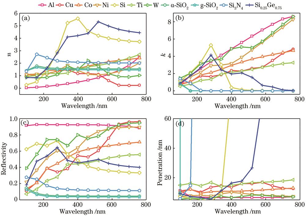
    Fig. 2. Comparison results of optical properties of various materials. (a) Refractive index; (b) extinction coefficient; (c) normal reflectivity; (d) penetration depth
    Scattering signal intensity of defects in the Cu pattern on a Si substrate under the varying spectral range
    Fig. 3. Scattering signal intensity of defects in the Cu pattern on a Si substrate under the varying spectral range
    Scattering signal intensity of defects under conventional and annular illumination configurations. (a) Bridge defect; (b) cutting-line defect; (c) particle defect
    Fig. 4. Scattering signal intensity of defects under conventional and annular illumination configurations. (a) Bridge defect; (b) cutting-line defect; (c) particle defect
    Conventional optical inspection methods for defects in the patterned wafer. (a) Bright-field inspection for defects; (b) dark-field inspection for defects; (c) schematic diagram of online defect inspection for the patterned wafer
    Fig. 5. Conventional optical inspection methods for defects in the patterned wafer. (a) Bright-field inspection for defects; (b) dark-field inspection for defects; (c) schematic diagram of online defect inspection for the patterned wafer
    TSOM for defect inspection. (a) Principle of TSOM[112]; (b) volumetric analysis for defect detection[75]
    Fig. 6. TSOM for defect inspection. (a) Principle of TSOM[112]; (b) volumetric analysis for defect detection[75]
    Phase-based optical inspection system for defects. (a) Epi-DPM[132]; (b) optical pseudo electrodynamics microscopy[137]
    Fig. 7. Phase-based optical inspection system for defects. (a) Epi-DPM[132]; (b) optical pseudo electrodynamics microscopy[137]
    Interferometric cross-polarization microscopy for defect inspection. (a) Schematic diagram of an interferometric cross-polarization microscopy [156]; (b) optical amplitude of the scattered light from the Au nanoparticle[156]; (c) optical phase difference with respect to the light in the reference branch [156]
    Fig. 8. Interferometric cross-polarization microscopy for defect inspection. (a) Schematic diagram of an interferometric cross-polarization microscopy [156]; (b) optical amplitude of the scattered light from the Au nanoparticle[156]; (c) optical phase difference with respect to the light in the reference branch [156]
    Characteristics of far-field diffraction patterns from Gaussian and OAM beams illuminating on blank substrate with amplitude-only defects[164]. (a)(b) Complex fields from the defect-free substrate and from the defect in the far-field from Gaussian CFS; (c) interference intensity pattern; (d) far-field diffraction pattern; (e)-(h) corresponding results of coherent Fourier scattering measurement based on ± 1 order orbital angular momentum beam
    Fig. 9. Characteristics of far-field diffraction patterns from Gaussian and OAM beams illuminating on blank substrate with amplitude-only defects[164]. (a)(b) Complex fields from the defect-free substrate and from the defect in the far-field from Gaussian CFS; (c) interference intensity pattern; (d) far-field diffraction pattern; (e)-(h) corresponding results of coherent Fourier scattering measurement based on ± 1 order orbital angular momentum beam
    THz detection method for defects in the wafer. (a) Schematic of THz wave-based defect inspection system; (b) schematic of THz real-time imaging system
    Fig. 10. THz detection method for defects in the wafer. (a) Schematic of THz wave-based defect inspection system; (b) schematic of THz real-time imaging system
    Defect inspection system for 3D NAND flash memory[185]. (a) Schematic of a standard optical-microscopy-based defect inspection system; (b) schematic of a typical 3D NAND flash memory structure; (c) near-infrared micrographs for several near-infrared-identified defect spots
    Fig. 11. Defect inspection system for 3D NAND flash memory[185]. (a) Schematic of a standard optical-microscopy-based defect inspection system; (b) schematic of a typical 3D NAND flash memory structure; (c) near-infrared micrographs for several near-infrared-identified defect spots
    EUV ptychography imaging-based defect inspection[197]. (a) Schematic of the amplitude- and phase-sensitive imaging reflectometer with large-area, spatially and depth-resolved capability; (b) original phase reconstruction from EUV ptychography imaging; (c) zoom-in of EUV ptychographic phase reconstructions of the sample after precision implementation of 3D tilted-phase correction and total variation regularization; (d) entire wide field-of-view amplitude reconstruction
    Fig. 12. EUV ptychography imaging-based defect inspection[197]. (a) Schematic of the amplitude- and phase-sensitive imaging reflectometer with large-area, spatially and depth-resolved capability; (b) original phase reconstruction from EUV ptychography imaging; (c) zoom-in of EUV ptychographic phase reconstructions of the sample after precision implementation of 3D tilted-phase correction and total variation regularization; (d) entire wide field-of-view amplitude reconstruction
    Multiple electron beam scanning detection system for defect inspection. (a) Schematic of the HMI-integrated MBI system; (b) upper part is the large field-of-view MBI images for wafer alignment, and the lower part is the MBI image of a periodic line/space pattern with a pitch of 46 nm, in which line-bridging and line-broken defects are contained in the pattern
    Fig. 13. Multiple electron beam scanning detection system for defect inspection. (a) Schematic of the HMI-integrated MBI system; (b) upper part is the large field-of-view MBI images for wafer alignment, and the lower part is the MBI image of a periodic line/space pattern with a pitch of 46 nm, in which line-bridging and line-broken defects are contained in the pattern
    Thermal imaging inspection for defects in the wafer. (a) Schematic diagram of wafer inspection system based on thermal effects; (b) structural schematic diagram of thermal detection unit; (c) a typical thermal profile image reported by the thermal detection unit[212]
    Fig. 14. Thermal imaging inspection for defects in the wafer. (a) Schematic diagram of wafer inspection system based on thermal effects; (b) structural schematic diagram of thermal detection unit; (c) a typical thermal profile image reported by the thermal detection unit[212]
    Quality improvement of the reference image[240]
    Fig. 15. Quality improvement of the reference image[240]
    D2DB method and the corresponding results[243]. (a) A trainable D2DB algorithm based on the convolutional neural networks; (b) central bridge defects detected by using the trainable D2DB algorithm under the conditions of 1 nm/pixel~4 nm/pixel (upper is aerial images of defective pattern with defect located in the yellow box, middle is enlarged view of defect feature located in the yellow box, bottom is test results)
    Fig. 16. D2DB method and the corresponding results243. (a) A trainable D2DB algorithm based on the convolutional neural networks; (b) central bridge defects detected by using the trainable D2DB algorithm under the conditions of 1 nm/pixel~4 nm/pixel (upper is aerial images of defective pattern with defect located in the yellow box, middle is enlarged view of defect feature located in the yellow box, bottom is test results)
    Summary and roadmap of patterned wafer defect inspection
    Fig. 17. Summary and roadmap of patterned wafer defect inspection
    Jiamin Liu, Hang Zhao, Qizhe Wu, Xianrui Feng, Xiangyu Zhao, Zhenyang Zhang, Chumiao Zhang, Tao Huang, Jinlong Zhu, Shiyuan Liu. Patterned Wafer Defect Inspection at Advanced Technology Nodes[J]. Laser & Optoelectronics Progress, 2023, 60(3): 0312003
    Download Citation