• Journal of Semiconductors
  • Vol. 41, Issue 4, 042601 (2020)
Jinyu Yang1, Yang Wang1, Lu Wang1, Ziao Tian2, Zengfeng Di2, and Yongfeng Mei1
Author Affiliations
  • 1Department of Material Science, Fudan University, Shanghai 200433, China
  • 2Shanghai Institute of Microsystem and Information Technology, Chinese Academy of Sciences, Shanghai 20050, China
  • show less
    DOI: 10.1088/1674-4926/41/4/042601 Cite this Article
    Jinyu Yang, Yang Wang, Lu Wang, Ziao Tian, Zengfeng Di, Yongfeng Mei. Tubular/helical architecture construction based on rolled-up AlN nanomembranes and resonance as optical microcavity[J]. Journal of Semiconductors, 2020, 41(4): 042601 Copy Citation Text show less
    (Color online) (a) TEM images from the cross section of an aluminum nitride nanomembrane. (b) High resolution TEM image of the AlN component in the nanomembrane. (c) X-ray diffraction pattern of the AlN component. (d) Schematic diagram of the fabrication process using rolled up technology. (e) SEM image of rolled-up tubular structures. inset: the cross-section of the tube (scale bar = 10 μm). (f) SEM image of rolled-up two helices with opposite direction.
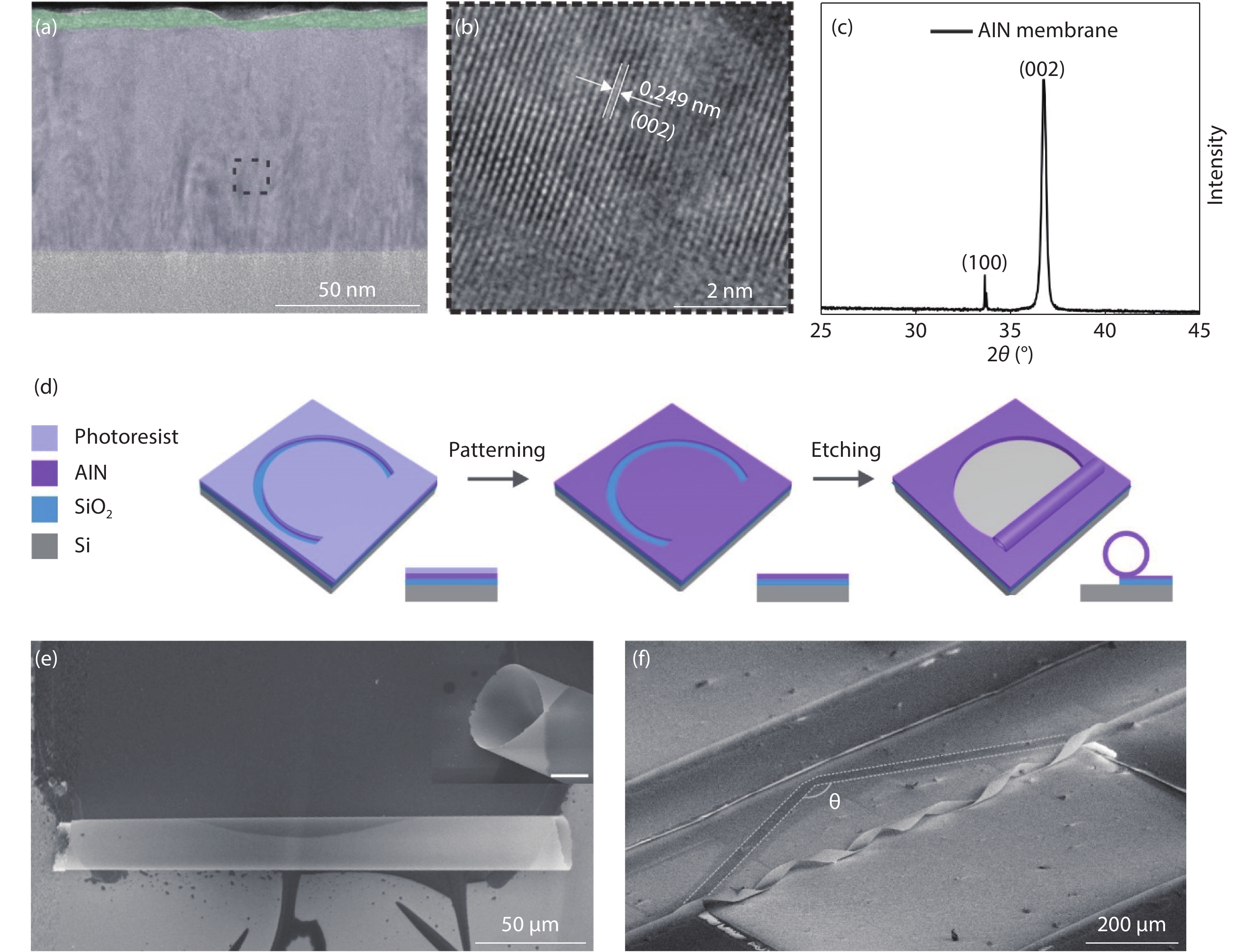
    Fig. 1. (Color online) (a) TEM images from the cross section of an aluminum nitride nanomembrane. (b) High resolution TEM image of the AlN component in the nanomembrane. (c) X-ray diffraction pattern of the AlN component. (d) Schematic diagram of the fabrication process using rolled up technology. (e) SEM image of rolled-up tubular structures. inset: the cross-section of the tube (scale bar = 10 μm). (f) SEM image of rolled-up two helices with opposite direction.
    (Color online) (a) Schematic diagram of V-shaped pattern. (b) SEM images of AlN helices structures fabricated from V-shaped patterns with different angles of 130°,140°,150°,160° (scale bar = 200 μm).
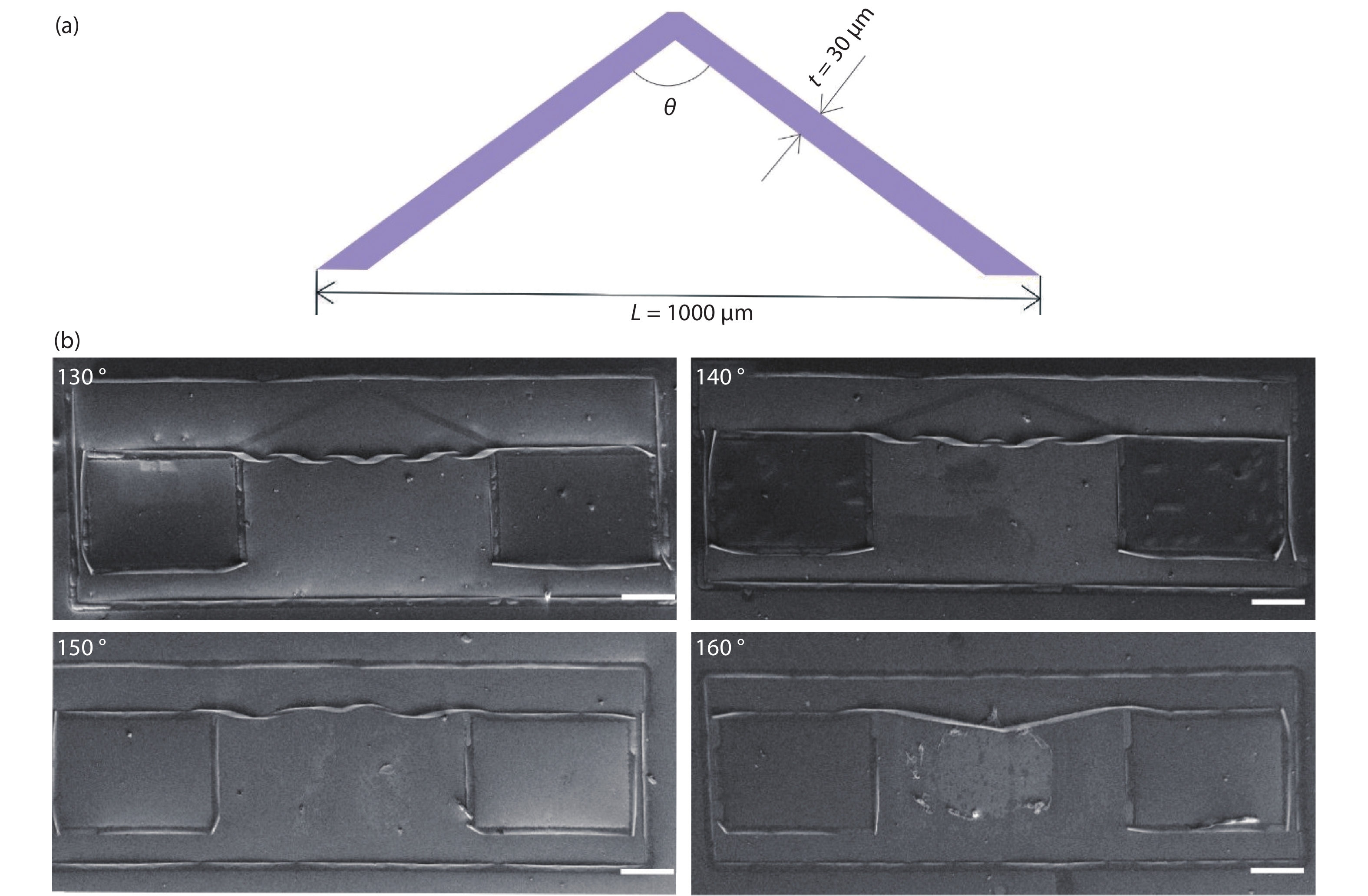
    Fig. 2. (Color online) (a) Schematic diagram of V-shaped pattern. (b) SEM images of AlN helices structures fabricated from V-shaped patterns with different angles of 130°,140°,150°,160° (scale bar = 200 μm).
    (Color online) (a) The diameter of a single tube as a function of the AlN membrane thickness after ICP-RIE etching. Insets show corresponding SEM images of microtubes with various diameters (scale bar = 10 μm). (b) Optical microscope image of ordered microtubes array from AlN NMs.
    Fig. 3. (Color online) (a) The diameter of a single tube as a function of the AlN membrane thickness after ICP-RIE etching. Insets show corresponding SEM images of microtubes with various diameters (scale bar = 10 μm). (b) Optical microscope image of ordered microtubes array from AlN NMs.
    (Color online) (a) Raman spectra of AlN before and after the rolling-up process. (b) Enlarged view of Raman peak shift. (c) Optical resonance of AlN microcavity before (blue line) and after (red line) the ALD process. Insets show corresponding SEM images of AlN microcavity before (scale bar = 20 μm) and after postprocess (scale bar = 30 μm). (d) Simulated mode positions as a function of tubes with various diameters (blue line and circle symbol). Experimental results showed as red star symbols.
    Fig. 4. (Color online) (a) Raman spectra of AlN before and after the rolling-up process. (b) Enlarged view of Raman peak shift. (c) Optical resonance of AlN microcavity before (blue line) and after (red line) the ALD process. Insets show corresponding SEM images of AlN microcavity before (scale bar = 20 μm) and after postprocess (scale bar = 30 μm). (d) Simulated mode positions as a function of tubes with various diameters (blue line and circle symbol). Experimental results showed as red star symbols.
    θ (°) 130140150160
    Pitch (μm) 200250333.3> 1000
    Number of turns2.521.5< 0.5
    Table 1. Statistical results of different helices.
    Jinyu Yang, Yang Wang, Lu Wang, Ziao Tian, Zengfeng Di, Yongfeng Mei. Tubular/helical architecture construction based on rolled-up AlN nanomembranes and resonance as optical microcavity[J]. Journal of Semiconductors, 2020, 41(4): 042601
    Download Citation