
Jinyu Yang, Yang Wang, Lu Wang, Ziao Tian, Zengfeng Di, Yongfeng Mei. Tubular/helical architecture construction based on rolled-up AlN nanomembranes and resonance as optical microcavity[J]. Journal of Semiconductors, 2020, 41(4): 042601
- Journal of Semiconductors
- Vol. 41, Issue 4, 042601 (2020)
Abstract
1. Introduction
Aluminum-nitride (AlN) is an interesting group III–V semiconductor, which presents direct band gap (around 6.2 eV), high thermostability, good piezoelectricity and high chemical stability[
Tubular optical microcavities can be fabricated through rolling-up nanotechnology[
In this work, two typical 3D structures including tubes and helices based on AlN NMs were constructed and WGMs in AlN microtubes were demonstrated and optimized. The good-quality AlN NMs were certified by the microstructural characterization involving the crystallinity and the lattice constant of AlN. Based on the decreased flexural rigidity of AlN NMs after thinning the membrane, the NMs self-assembly transformed into 3D structures via rolled-up nanotechnology. Tubes with various diameters were constructed by controlling the thickness of NMs, and the strain variation before and after the rolling-up process were characterized by a micro-Raman device, which corresponded to the theoretical predication. The WGMs mode was also observed in AlN-based optical microcavities by photoluminescence spectrum. Postprocesses, including atomic layer deposition and R6G immersion, were employed on as-fabricated AlN tubes to promote the quality factor (Q-factor).
2. Experimental details
2.1. Growth and characterization of AlN NMs
In this work, the AlN NMs were grown on the Si-on-insulator wafer (SOI wafer, with 1 μm SiO2 top layer) via magnetron sputtering with a nominal thickness of 80 nm provided by Prefab company. The as-grown AlN NMs were then cleaned by ultra-sonication in acetone, ethanol and deionized water for 5 min. After cleaning, the microstructure and element mapping of AlN were characterized by transmission electron microscopy (TEM, FEI TECNAI G2 S-TWIN F20). Before the characterization by TEM, the sample preparation was conducted via focused ion beam (FIB, FEI Helios NanoLab 600). The surface morphology was characterized by atomic force microscope (AFM, BRUKER Dimension Icon). The crystallinity information was given by an X-Ray diffraction device (XRD, BRUKER D8A Advance).
2.2. Fabrication of AlN 3D structures
The photolithography process is a common method to pattern the NMs in the rolling-up process, the AlN 3D structures in this work were constructed utilizing pre-defined patterns. Firstly, a layer of photoresist (AZ5214) was spin-coated on the cleaned AlN NMs at a speed of 4000 r/min. Then, the plate making machine (Heidelberg Upg501) was utilized to create pre-defined patterns on the AlN NMs. The exposure photoresist and the AlN layer downward could be removed by the developing liquid (TMAH, from RuiHong Inc.) simultaneously. Finally, the patterned AlN NMs were rinsed in ethanol to remove the photoresist.
After patterning of AlN NMs, the sample was immersed in a 40% HF solution to selectively remove the sacrificial layer (SiO2). During the etching process, the top AlN layer released and detached from the substrate. The released NMs then self-assembly roll-up into different 3D structures according to pre-defined patterns and the intrinsic strain in the membrane.
2.3. Thinning process of AlN membrane
Inductively coupled plasma-reactive ion etching (ICP-RIE) was employed to thin the AlN membrane, the parameters used in this work were: 25 sccm total gas flow (20 sccm BCl3, 5 sccm Ar for stabilization), 20 °C electrode temperature, 30–60 s etching time, 20 mT total pressure, 1000 W ICP power, and a dc-bias of 250 ± 10 V.
2.4. Characterization of AlN microcavities
The morphological property of the as-fabricated AlN structures were characterized via scanning electron microscopy (SEM, JEOL JSM-6701F). Additionally, the micro-Raman scattering spectroscopy (Horiba JY HR-800) with the 532 nm laser as the excitation source was utilized to analyze the strain distribution and optical resonances in AlN microcavities.
3. Results and discussion
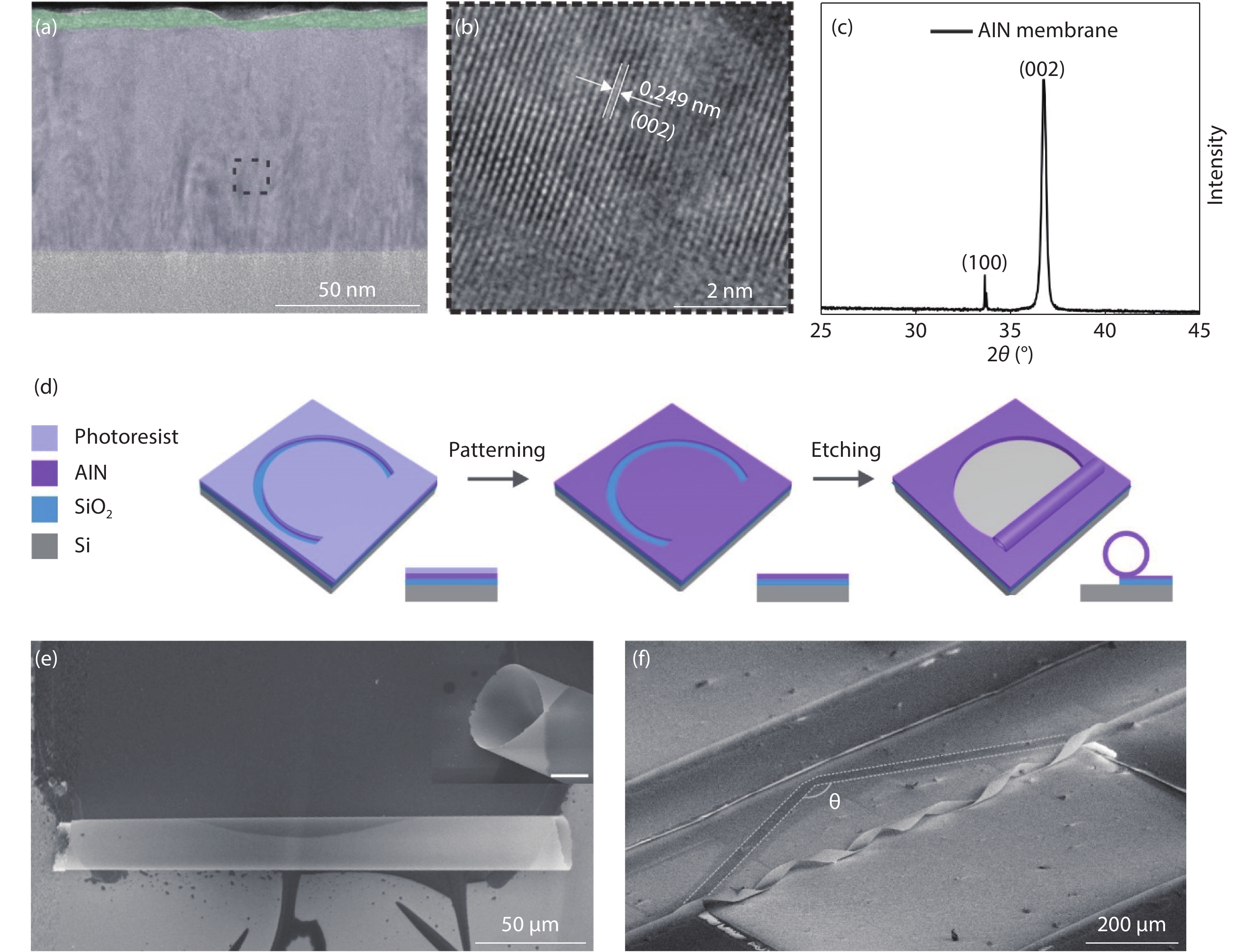
Fig. 1(a) shows the TEM image of AlN NMs, including three layers: AlN layer with thickness of 80 nm, SiO2 layer with thickness of 1 μm, and Si layer (not shown in Fig. 1(a)). As well, another layer with thickness of 5 μm, showing amorphous microstructure, was observed above the AlN layer (the green region in Fig. 1(a)). We concluded that it is the oxidation of AlN because condensed O element distribution was confirmed in the layer according to element mapping results (shown in Fig. S1). Fig. 1(b) shows the polycrystalline structure and the main growth direction of AlN NMs with high resolution TEM (HRTEM), the lattice constant of 0.249 nm is corresponding to the (002) plane. XRD pattern of polycrystalline AlN is given in Fig. 1(c). Two peaks near 33.22° and 36.04° could be attributed to (100) and (002) planes of AlN, respectively. The surface morphology of AlN NMs was characterized by atomic force microscope (AFM), as shown in Fig. S2. Columnar structures with pointed tips, or cone structures are in accordance with morphology results in previous work on N-polar AlN[
![]()
Figure 1.(Color online) (a) TEM images from the cross section of an aluminum nitride nanomembrane. (b) High resolution TEM image of the AlN component in the nanomembrane. (c) X-ray diffraction pattern of the AlN component. (d) Schematic diagram of the fabrication process using rolled up technology. (e) SEM image of rolled-up tubular structures. inset: the cross-section of the tube (scale bar = 10
Fig. 1(d) shows the fabrication process of AlN tubular structures. Photolithography was used to pattern the AlN NMs. Different from other materials which need another step to create the etching window on the NMs[
For AlN polycrystalline membranes with isotropic strain, the rolled-up structures are mainly decided by pre-defined pattern and strain gradient. In this work, two helices of opposite chirality were constructed from V-shaped patterns (marked as the grey dotted lines in Fig. 1(f)). The rolling-up direction of two stripes present competitive behavior, thus this kind of pattern has excellent controllability on helices formation. Moreover, for V-shaped patterns with constant length and width, the helices pitch and the number of turns could be tuned through the angle θ between two stripes (marked as the grey curve in Fig. 1(f)). The statistical results are given in Table 1 (the SEM images of different helices are shown in Fig. 2).
![]()
Figure 2.(Color online) (a) Schematic diagram of V-shaped pattern. (b) SEM images of AlN helices structures fabricated from V-shaped patterns with different angles of 130°,140°,150°,160° (scale bar = 200
The pitch increases and the number of turns decreases with increasing θ, which can be explained by limit hypothesis. When θ is limited to zero, two stripes overlap and the competition disappeared, and they will roll-up into the tube which pitch is 0; when θ is limited to 180°, two separate stripes could be considered as a straight stripe with large pitch. The helices in Fig. 1(f) is constructed from V-shaped pattern with θ of 130°. Actually, AlN with (002) crystal orientation also presents piezoelectricity[
Two parameters which could control the diameter of rolled-up tubes are strain gradient and layer thickness[
where tstrain and trelax are the respective thickness of the compressive and relaxed strain layers, m = tstrain/trelax is their ratio, Δε is the strain difference between two layers which could be calculated form Raman shift[
![]()
Figure 3.(Color online) (a) The diameter of a single tube as a function of the AlN membrane thickness after ICP-RIE etching. Insets show corresponding SEM images of microtubes with various diameters (scale bar = 10
To clarify the strain gradient in the membrane, micro-Raman device was adopted to AlN NMs before and after the rolling-up process, as shown in Figs. 4(a) and 4(b). Fig. 4(a) shows Raman spectra of as-grown and rolled-up AlN NMs under an excitation laser wavelength of 532 nm. AlN features three Raman peaks in the detectable regime, i.e., the A1(TO), E2(high), and A1(LO). Among them, E2(high) shows a higher sensitivity to strain variation, thus commonly it is utilized as a symbol to analyze the membrane states[
![]()
Figure 4.(Color online) (a) Raman spectra of AlN before and after the rolling-up process. (b) Enlarged view of Raman peak shift. (c) Optical resonance of AlN microcavity before (blue line) and after (red line) the ALD process. Insets show corresponding SEM images of AlN microcavity before (scale bar = 20
The linear relationship between stress variation and E2(high) shift has been investigated in previous reports[
Δω is the linear coefficient –2.9 (cm–1/GPa), ω0 is the E2(high) peak position in the relaxed membrane and ω is in the stressed state, σ is the intrinsic stress. Combining with the experiments, stress in the as-grown membrane calculated from this equation is –613 MPa (– means the stress in the membrane is compressive). Stress in the rolled-up membrane is +517 MPa (+ means the stress is tensile). Strain could be deduced from stress with Yong’s modulus.
Eventually, the optical characterization of AlN microcavities was carried out via photoluminescence (PL) measurements. The result is given in Fig. 4(c) (marked as a blue line), AlN microcavity fabricated from rolling-up technology presented a stable WGM mode in the range of 580–600 nm. Actually, the band gap of AlN is around 6.2 eV, which, in theory, couldn’t be excited by 532 nm wavelength laser. However, the impurity introduction couldn’t be prohibited totally in the membrane growth process in reality. From the element mapping result (given in Fig. S1), uniform oxygen element distribution was observed in the AlN region, which indicates that defects like oxygen point defects (
The Q-factor could be calculated from the equation
where λ is the resonant wavelength, Δλ is the FWHM corresponding to the full width at half maximum of the resonant peak. The calculated result shows the Q-factor of as-fabricated AlN microcavities is around 200, which is at medium level among rolled-up tubular resonators, such as SiOx/Si (Q < 100), GaN ( Q ~ 100), and Y2O3/ZrO2 (Q > 1500) [
where Δ is the wall thickness, σ is the material conductivity, ε0 is the vacuum dielectric constant and ω is the angular frequency. The neff could be divided into a real part and an imaginary parti, and the imaginary part was used to evaluate the light loss. With Δ increased, the imaginary part decreased and the light loss in the propogation process will reduce. In other words, the Q factor increased. Lin[
Tubes with different diameters have been fabricated in the last section, then the resonance peak shifts caused by the diameter variation was further investigated. Simulation by finite element methods is given in Fig. 4(d) (blue line and circle symbol). For a given mode, the resonance shifted to longer wavelength with increasing the diameter of tube. Experiments result (red star symbols in Fig. 4(d)) is consistent with the simulation.
4. Conclusion
In conclusion, AlN tubular micro-resonator were fabricated by rolling up AlN NMs grown on SOI. Microstructural characterization demonstrated that the AlN main growth direction is (002). The thickness and the stiffness of AlN NMs were reduced through ICP-RIE process, the thickness was tuned to 40, 60, and 80 nm respectively, then AlN tubes with different diameters (d = 15, 21, and 29 μm) were fabricated. Stress distributions of the as-grown and the rolled-up AlN membrane were characterized via micro-Raman spectroscopy and specific values of stress were deduced from the Stress–Raman shift formula. The calculation results show that the membrane stress was shifted from –613 to +517 MPa after rolling up process (– means the compressive stress, + means the tensile stress). Micro-Raman measurements showed the resonant behavior of as-fabricated AlN micro-cavities clearly, and the Q-factor reached 193. Postprocess was utilized to improve the Q-factor to 291, which advancement could be explained by tube refractive index increment. Such AlN micro-resonators based on tubular microcavities offer a novel design route for Si-based integrated light source. Moreover, the rolled-up technology provides a new possibility for AlN 3D structures fabrication, which is promising for AlN application in MEMS and photonics fields.
Acknowledgments
This work was supported by the National Natural Science Foundation of China (Nos. 61905270, 51961145108), Natural Science Foundation of Shanghai (19ZR1467100), Science and Technology Commission of Shanghai Municipality (17JC1401700), and the Program of Shanghai Academic Research Leader (19XD1400600).
References
[1] I Vurgaftman, J R Meyer, L R Ram-Mohan. Band parameters for III–V compound semiconductors and their alloys. J Appl Phys, 89, 5815(2001).
[2] L W Li, Y Bando, Y C Zhu et al. Single-crystalline AlN nanotubes with carbon-layer coatings on the outer and inner surfaces via a multiwalled-carbon-nanotube-template-induced route. Adv Mater, 17, 213(2005).
[3] C R Bowen, H A Kim, P M Weaver et al. Piezoelectric and ferroelectric materials and structures for energy harvesting applications. Energy Environ Sci, 7, 25(2013).
[4] B J Zheng, W Hu. Cubic AlN thin film formation on quartz substrate by pulse laser deposition. J Semicond, 37, 063003(2016).
[5] N Sinha, G E Wabiszewski, R Mahameed et al. Piezoelectric aluminum nitride nanoelectromechanical actuators. Appl Phys Lett, 95, 053106(2009).
[6] C Xiong, W H P Pernice, X Sun et al. Aluminum nitride as a new material for chip-scale optomechanics and nonlinear optics. New J Phys, 14, 095014(2012).
[7] S Longhi, L Feng. Unidirectional lasing in semiconductor microring lasers at an exceptional point. Photonics Res, 5, B1(2017).
[8] M Bürger, M Ruth, S Declair et al. Whispering gallery modes in zinc-blende AlN microdisks containing non-polar GaN quantum dots. Appl Phys Lett, 102, 081105(2013).
[9] J Wang, T Zhan, G Huang et al. Optical microcavities with tubular geometry: properties and applications. Laser Photonics Rev, 8, 521(2014).
[10] X Lin, Y Fang, L Zhu et al. Self-rolling of oxide nanomembranes and resonance coupling in tubular optical microcavity. Adv Opt Mater, 4, 936(2016).
[11] T Kipp, H Welsch, C Strelow et al. Optical modes in semiconductor microtube ring resonators. Phys Rev Lett, 96, 077403(2006).
[12] G Huang, Y Mei. Assembly and self-assembly of nanomembrane materials—from 2D to 3D. Small, 14, 1703665(2018).
[13] Z Tian, L Zhang, Y Fang et al. Deterministic self-rolling of ultrathin nanocrystalline diamond nanomembranes for 3D tubular/helical architecture. Adv Mater, 29, 1604572(2017).
[14] G S Huang, Y F Mei, F Cavallo et al. Fabrication and optical properties of C/
[15] X Yu, W Huang, M Li et al. Ultra-small, high-frequency, and substrate-immune microtube inductors transformed from 2D to 3D. Sci Rep, 5, 9661(2015).
[16] Y Fang, Xn Li, S Tang et al. Temperature-dependent optical resonance in a thin-walled tubular oxide microcavity. Prog Nat Sci Mater, 27, 498(2017).
[17] C Yan, W Xi, W Si et al. Highly conductive and strain-released hybrid multilayer Ge/Ti nanomembranes with enhanced lithium-ion-storage capability. Adv Mater, 25, 539(2013).
[18] J Kim, U Choi, J Pyeon et al. Deep-ultraviolet AlGaN/AlN core-shell multiple quantum wells on AlN nanorods via lithography-free method. Sci Rep, 8, 935(2018).
[19] G Huang, Y Mei. Thinning and shaping solid films into functional and integrative nanomembranes. Adv Mater, 24, 2517(2012).
[20] M Akiyama, Y Morofuji, T Kamohara et al. Flexible piezoelectric pressure sensors using oriented aluminum nitride thin films prepared on polyethylene terephthalate films. J Appl Phys, 1143185(2006).
[21] C Zhao, K E Knisely, D J Colesa et al. Voltage readout from a piezoelectric intracochlear acoustic transducer implanted in a living guinea pig. Sci Rep, 9, 3711(2019).
[22] N Ledermann, P Muralt, J Baborowski et al. Piezoelectric Pb(Zr
[23] P Froeter, X Yu, W Huang et al. 3D hierarchical architectures based on self-rolled-up silicon nitride membranes. Nanotechnology, 24, 475301(2013).
[24] B W Dodson, J Y Tsao. Relaxation of strained-layer semiconductor structures via plastic flow. Appl Phys Lett, 51, 1325(1987).
[25] H J Trodahl, F Martin, P Muralt et al. Raman spectroscopy of sputtered AlN films: E2 (high) biaxial strain dependence. Appl Phys Lett, 89, 061905(2006).
[26] I Yonenaga, T Shima, M H F Sluiter. Nano-indentation hardness and elastic moduli of bulk single-crystal AlN. Jpn J Appl Phys, 41, 4620(2002).
[27] M Kuball, J M Hayes, A D Prins et al. Raman scattering studies on single-crystalline bulk AlN under high pressures. Appl Phys Lett, 78, 724(2001).
[28] Y Tang, H Cong, F Li et al. Synthesis and photoluminescent property of AlN nanobelt array. Diamond Relat Mater, 16, 537(2007).
[29] Y G Cao, X L Chen, Y C Lan et al. Blue emission and Raman scattering spectrum from AlN nanocrystalline powders. J Cryst Growth, 213, 198(2000).
[30] J Wang, E Song, C Yang et al. Fabrication and whispering gallery resonance of self-rolled up gallium nitride microcavities. Thin Solid Films, 627, 77(2017).
[31] J Wang, T Zhang, G Huang et al. Tubular oxide microcavity with high-indexcontrast walls: Mie scattering theory and 3D confinement of resonant modes. Opt Express, 20, 18555(2012).

Set citation alerts for the article
Please enter your email address
© Copyright 2018-2021 | Chinese Laser Press. All Rights Reserved 沪ICP备15018463号-20