
Jia-Bin LI, Xiao-Hua WANG, Wen-Jie WANG. Modulation of the optical properties of GaN(0001) surface by metal atom adsorption[J]. Journal of Infrared and Millimeter Waves, 2020, 39(6): 671
- Journal of Infrared and Millimeter Waves
- Vol. 39, Issue 6, 671 (2020)
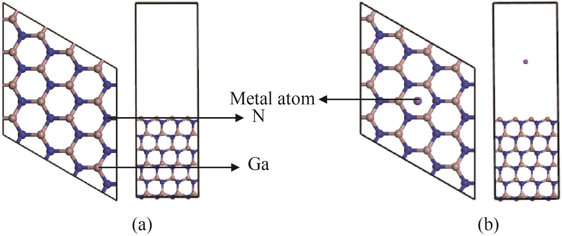
Fig. 1. The 4×4×3 structures of (a) pristine GaN(0001) surface, and (b) GaN(0001) surface adsorbed with metal atom. (Adatoms occupy the center of the hexagon)
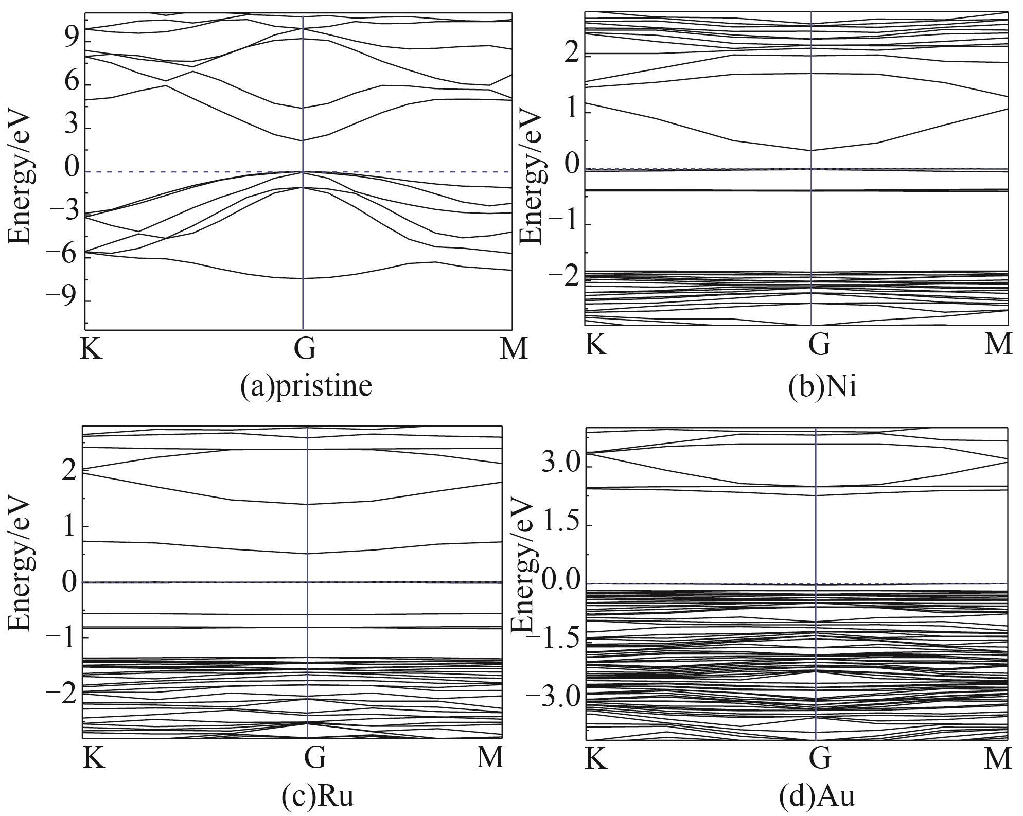
Fig. 2. Energy band structures of (a) pristine GaN(0001) surface, and(b-d) GaN(0001) surface absorbed with different metal atoms. The blue solid lines represent G point of the Brillouin zone, the blue dashed line at 0 eV represents the Fermi level
Fig. 3. PDOS of (a)pristine GaN(0001) surface, and (b-d) GaN(0001) surface absorbed with different metal atoms. The dashed line at 0 eV represents the Fermi level
Fig. 4. Optical properties of GaN(0001) surface absorbed with different metal atoms (a) real part of dielectric function, (b) imaginary part of dielectric function, (c) absorption, (d) loss function, (e) reflectivity, and (f) real part of refractive index
|
Table 1. Binding energies of atoms adsorbed on the GaN(0001) surface (Eb in eV)
|
Table 2. Number of transferred charges between the adatoms and GaN(0001) surface. Positive values represent that charges transfer from adatoms to GaN(0001) surface
| ||||||||||||||||||||||||||||||||||||||||||||
Table 3. Key parameters of the pristine GaN(0001) surface and the GaN(0001) surface adsorbed with different metal atoms

Set citation alerts for the article
Please enter your email address
© Copyright 2018-2021 | Chinese Laser Press. All Rights Reserved 沪ICP备15018463号-20