
Jia-Bin LI, Xiao-Hua WANG, Wen-Jie WANG. Modulation of the optical properties of GaN(0001) surface by metal atom adsorption[J]. Journal of Infrared and Millimeter Waves, 2020, 39(6): 671
- Journal of Infrared and Millimeter Waves
- Vol. 39, Issue 6, 671 (2020)
Abstract
Introduction
GaN material occupies an important position in modern electronic and optoelectronic devices due to its advantages such as wide bandgap, excellent transmission characteristics, and the wavelength range from near infrared band to near ultraviolet band. GaN has low electron affinity, which can be used as field emission electron source. GaN based blue and green LED (light-emitting diode) and laser diode can be realized due to its wide direct bandgap[
Substitutional doping has been widely used to modulate the properties of GaN. For example, GaN exhibits p-type semiconductor characteristics by Be or Mg doping, and GaN exhibits n-type semiconductor characteristics by Si doping[
In this study, different metals (Ni, Ru, and Au) that are commonly used in experiments are selected to adsorb on the GaN(0001) surface to tune its photoelectric properties through the first principles calculation. The optical properties have been investigated through the hybridization of electronic states and the electron transition theory. Collectively, the results may well provide an especially useful framework for the application of GaN(0001) surface in optoelectronic field.
1 Computational detail
In this paper, the Cambridge Sequential Total Energy Package (CASTEP) module is adopted to calculate the electronic structure, work function, and optical properties of metal atom adsorbed GaN(0001). Simulations are performed under generalized gradient approximation (GGA) with Perdew-Burke-Ernzerhof (PBE) exchange and correlation. In the process of structure optimization, 450eV mesh cutoff energy is set for the expansion of plane wave basis sets and the convergence criteria is set to 5×10⁻⁶ eV for all systems. The Brillouin-zone (BZ) integration is calculated by the highly symmetric K points in the form of a Monkhorst-Pack 9×9×1 grid. The convergence criterion of the interaction force between atoms is set to 0.02 eV, and the stress convergence criterion in the crystal is set to 0.1 GPa. The convergence criterion of the maximal displacement of atoms is 1×10⁻³ Å. All calculations are carried in reciprocal space with Ga 4s24p1, N 2s22p3, Ni 3d84s2, Ru 4d75s1, and Au 5d106s1 as the valence electrons.
2 Results and discussion
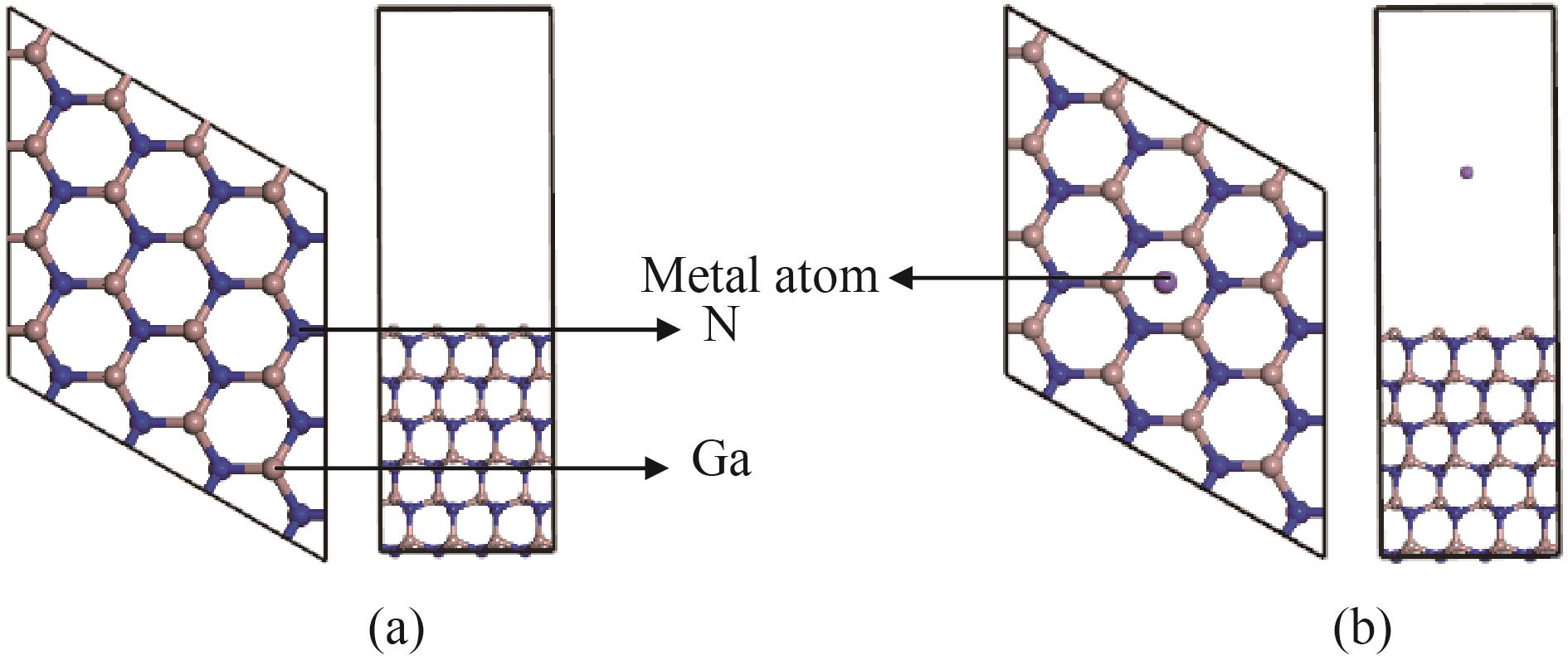
A 4×4×3 supercell of the GaN(0001) surface structure is constructed as shown in Fig. 1(a), the top two layers of this model are relaxed freely, the bottom four layers are fixed. 30 Å vacuum region perpendicular to the GaN(0001) surface is added, which is verified to be wide enough (based on the average electrostatic potential plot).The boundary conditions are set to be periodic. For the GaN(0001) surface, the hollow sites (at the center of a hexagon), the top of gallium atom, the top of nitride atom, and the center of bridge between gallium and nitride atoms are the possible adsorption sites. The GaN(0001) surface structures with adatoms occupying different adsorption sites are optimized, the results show that the adatoms prefer to occupy the hollow site of the GaN(0001) surface. Thus, the following discussions are all with respect to the GaN(0001) surface structure with adatoms occupying hollow adsorption site as shown in Fig.1(b).
![]()
Figure 1.The 4×4×3 structures of (a) pristine GaN(0001) surface, and (b) GaN(0001) surface adsorbed with metal atom. (Adatoms occupy the center of the hexagon)
For the GaN(0001) surface adsorbed with metal atom, the vertical distance between the adatom and the GaN(0001) surface is an important parameter. When the vertical distance between the adatom and the GaN(0001) surface is much longer than the bond length between N and Ga, there is no interaction between the adatom and the GaN(0001) surface. The vertical distance between the atoms and the GaN(0001) surface is less than the bond length between N and Ga, the bond length between N and Ga below the adatom increases as the adsorption distance decreases, the interaction between adatom and GaN(0001) surface is enhanced so that more charges transfer between them, the strength of orbital hybridization at the Fermi level of the GaN(0001) surface is enhanced at the same time. When the vertical distance between the adatom and the GaN(0001) surface is much smaller than the bond length between the N and Ga, the adatom will be transferred to the GaN(0001) surface, thus the GaN(0001) surface structure is destroyed. Taking the above results into consideration, the vertical distance between adatoms and the GaN(0001) surface is set to 2 nm.
The binding energy of atoms adsorbed on the GaN(0001) surface can be defined as:
where EGaN-nM is the total energy of the GaN(0001) surface adsorbed with metal atoms, EGaN is the total energy of the GaN(0001) surface, EM is the total energy of the free metal adatom, and n corresponds to the number of metal adatoms. The calculated binding energies of atoms adsorbed on the GaN(0001) surface are shown in Table 1. It is seen that all the binding energies of these adatoms are negative, indicating that these adsorption processes are exothermic, and the adsorption structures are stable. These results are like to those of adsorption structures of the GaN film presented in Ref. 36. The ionization potential is one of the most important factors that determine the binding energy of atom adsorbed on the GaN(0001) surface. The larger ionization potential of metal atom corresponds to the larger absolute value of the binding energy of atom adsorbed on the GaN(0001) surface. Among the three adatoms, Ni has the largest ionization potential and corresponds to the largest absolute value of the binding energy.
| Adatom | Ni | Ru | Au |
|---|---|---|---|
| Binding energy (Eb/eV) | -84.4 | -80.0.6 | -82.2 |
Table 1. Binding energies of atoms adsorbed on the GaN(0001) surface (Eb in eV)
Charge transfer is another important feature in the adsorption process. The number of transferred charges is presented in Table 2. As seen, all the adatoms loss the electrons due to the fact that their electronegativity is smaller than that of Ga atom. In the case of the GaN(0001) surface adsorbed with Ni and Ru, relatively notable electrons transfer from adatoms to GaN(0001) surface, suggesting significant chemical interaction between the adatoms and the GaN(0001) surfaces. For the GaN(0001) surface adsorbed with Au, small number of charges transfer from adatoms to GaN(0001) surface, which implies that weak interactions occur between adatoms and the GaN(0001) surface. The large charge transfer corresponds to strong interactions between the adatoms and the GaN(0001) surface, resulting in strong orbital hybridization between the adatoms and the GaN(0001) surfaces at the Fermi level, thus the work function of the GaN(0001) surface can be reduced.
| Adatoms | Ni | Ru | Au |
|---|---|---|---|
| Number of transferred charges | 0.27 | 0.26 | 0.05 |
Table 2. Number of transferred charges between the adatoms and GaN(0001) surface. Positive values represent that charges transfer from adatoms to GaN(0001) surface
Figure 2(a) shows the energy band structure of the pristine GaN(0001) surface. The direct band gap of the pristine GaN(0001) surface is observed, as well as the conduction band minimum (CBM) and the valence band maximum (VBM) locate at the G point in the Brillouin zone; the band gap Eg is 2.217eV, corresponding to the results shown in Ref. 37. Figures 2(b-d) show the energy band structures of the GaN(0001) surface adsorbed with different metal atoms. In the case of the GaN(0001) surface adsorbed with Ni, the direct but significantly reduced band gap is observed, the band gap is 0.32 eV. Some impurity energy levels below the Fermi level in the band gap are introduced, the smaller energy difference between impurity energy levels, impurity energy level and CBM, impurity energy level and VBM are also observed. The case of the GaN(0001) surface adsorbed with Ru is similar to that of the GaN(0001) surface adsorbed with Ni, the band gap is 0.001 eV, some impurity energy levels below and above the Fermi level in the band gap are observed. For the GaN(0001) surface adsorbed with Au, an impurity energy level that passes through the Fermi level is observed. The energy difference between impurity energy level and CBM (VBM) is 2.26 eV (0.15 eV), which is smaller than the band gap of pristine GaN(0001) surface. The reduction of energy difference between energy levels due to the adsorption of metal atoms on the GaN(0001) surface reduces the barrier height of carrier transition and facilitates the inter-band transition.
![]()
Figure 2.Energy band structures of (a) pristine GaN(0001) surface, and(b-d) GaN(0001) surface absorbed with different metal atoms. The blue solid lines represent G point of the Brillouin zone, the blue dashed line at 0 eV represents the Fermi level
Figure 3 shows the partial density of states (PDOS) of the pristine GaN(0001) surface and GaN(0001) surface adsorbed with different metal atoms. From Fig.3(a) we can see that the valence band of pristine GaN(0001) surface is divided into the upper valence band and the lower valence band from left to right, the Fermi level is located at the edge of the upper valence band. From Figs.3(b-d) we can see that orbital hybridization between adatoms and GaN(0001) surface at the Fermi levels takes place, the types of orbitals involved in hybridization and the intensity of orbital hybridization vary due to the adsorption of different metal atoms on the GaN(0001) surface. Charges transfer occurs between adatoms and GaN(0001) surface simultaneously, all the adatoms loss electrons due to their smaller ionization potential than that of Ga atom. In the case of the GaN(0001) surface adsorbed with Ni, strong orbital hybridization takes place between the 3d state orbits of Ni and the 2p states orbits of N at the Fermi level, 0.27 electrons transfer from the 3d state orbits of Ni to the GaN(0001) surface. In the case of the GaN(0001) surface adsorbed with Ru, strong orbital hybridization between the 4d state orbits of Ru and the 2p state orbits of N at the Fermi level also is observed, 0.26 electrons transfer from the 4d state orbits of Ru to the GaN(0001) surface. For the GaN(0001) surface adsorbed with Au, weak orbital hybridization takes place between the 6s state orbits of Au and the 2p state orbits of N at the Fermi level, 0.05 electrons transfer from the 6s state orbits of Au to the GaN(0001) surface. The strength of orbital hybridization between adatoms and the GaN(0001) surface represents the chemical interaction between them, the work function of GaN(0001) surface can be reduced by stronger orbital hybridization.
![]()
Figure 3.PDOS of (a)pristine GaN(0001) surface, and (b-d) GaN(0001) surface absorbed with different metal atoms. The dashed line at 0 eV represents the Fermi level
The work function (Φ) is an important parameter to determine the photoelectric properties of materials. Lower work function can improve the photoelectric properties of materials to some extent. The work function of any material can be defined as the energy required to remove an electron from the highest filled level in the Fermi distribution of a solid to vacuum at absolute zero. The calculated Φ of the pristine GaN(0001) surface is 4.483eV, which is in good agreement with the experimental value of (4.0 ± 0.2) eV [38] and close to the calculated result of 4.42 eV in Ref. 39. The work functions of the GaN(0001) surface adsorbed with different adatoms are 3.43 eV (Ni), 3.77 eV (Ru), and 5.29 eV (Au) respectively. It is seen that some metal atoms adsorption can reduce the work function of GaN(0001) surface while other metal atoms adsorption cannot. The increase or decrease of the work function of GaN(0001) surface depends on the electronegativity of the adatoms with respect to the Ga atom. In the case of the GaN(0001) surfaces adsorbed with Ni and Ru, the electronegativity of the adatoms is smaller than that of Ga atom. The surface dipole moment will be formed due to the interaction between adatoms and GaN(0001) surface, which reduces the work function of GaN(0001) surface. For the GaN(0001) surfaces adsorbed with Au, the work function is bigger than that of pristine GaN(0001) surface due to the bigger electronegativity of Au atom. Furthermore, the strength of orbital hybridization between adatoms and GaN(0001) surface at the Fermi levels has an indirect influence on the reduction of work function of GaN(0001) surface. From the analysis of PDOS of GaN(0001) surface adsorbed with metal atoms above we know that strong orbital hybridization takes place between Ni or Ru and the GaN(0001) surface at the Fermi level, which corresponds to the smaller work function of GaN(0001) surface.
The optical constants, relating the microscopic model of physical process with the microelectronic structure of the solid that can better characterize the physical properties of the material, are mainly determined by the electronic structures and the carrier concentration near the Fermi level. The changes of the electronic structures of GaN(0001) surface caused by the adsorption of different metal atoms would influence its optical properties. Figures 4(a-b) represent the frequency dependent real and imaginary parts of dielectric function ɛ(ω) of the pristine GaN(0001) surface and the GaN(0001) surface adsorbed with different metal atoms. ɛ1(ω) represents the real part of dielectric function, ɛ2(ω) represents the imaginary part of dielectric function. For the pristine GaN(0001) surface, the static dielectric function ɛ1(0) is found to be 3.44, six main peaks are observed in the graph of ɛ2(ω) at photon energy of 2.29 eV, 6.84 eV, 8.85 eV, 10.82 eV, 13.13 eV, and 17.51 eV. The peak at 2.29 eV corresponds to the transition of carriers from N 2p state orbit at VBM to Ga 4s state orbit or Ga 4p state orbit at CBM; the peak at 6.84 eV indicates the transition of carriers from Ga 4s state orbit within the upper valence band to Ga 4p state orbit within the conduction band; the peak at 8.56eV indicates the transitions of carriers from N 2p state orbit within the upper valence band to Ga 4s state orbit or Ga 4p state orbit within the conduction band; the peak at 10.82 eV corresponds to the transitions of carriers from Ga 3d state orbit within the lower valence band to N 2p state orbit within the upper valence band; the peak at 13.13 eV corresponds to the transitions of N 2s state (lower valence band) to N 2p state (upper valence band); the peak at 17.51 eV corresponds to the transitions of carriers from N 2s state orbit within the lower valence band to Ga 4s state orbit or Ga 4p state orbit within the conduction band. In the case of the GaN(0001) surface adsorbed with Ni, ɛ1(0) is found to be 2.94, which is smaller than that of pristine GaN(0001) surface. In the case of the GaN(0001) surfaces adsorbed with Ru and Au, ɛ1(0) is found to be 6.25 and 4.21 respectively, which are bigger than that of pristine GaN(0001) surface. From Fig.4(b) we can see that the numbers and the positions of the peaks in ɛ2(ω) that represent the transition of carriers change significantly. The peaks at 0 eV in ɛ2(ω) for all the GaN(0001) surfaces adsorbed with different metal atoms are observed, which represent the orbital hybridization between adatoms and GaN(0001) surface at the Fermi levels. Two peaks close to each other in the lower photon energy region are also observed, which correspond to the transitions of carriers between Ni 3d, Ru 4d, and Au 6s state orbits and Ga 4p, N 2p state orbits.
![]()
Figure 4.Optical properties of GaN(0001) surface absorbed with different metal atoms (a) real part of dielectric function, (b) imaginary part of dielectric function, (c) absorption, (d) loss function, (e) reflectivity, and (f) real part of refractive index
Figure 4(c) shows the absorption coefficients of the pristine GaN(0001) surface and the GaN(0001) surface adsorbed with different metal atoms. For the pristine GaN(0001) surface, the maximum value of the absorption coefficient is 21.3 μm-1 at the photon energy of 10.82 eV. The absorption edge begins at the photon energy of 2.29 eV, which corresponds to the direct transition threshold of carriers (VBM to CBM) and is in agreement with Ref. 40. For the GaN(0001) surface adsorbed with different metal atoms, the absorption intensity of light has changed a lot; the shrinkage phenomenon of the absorption curve in the high photon energy region is observed, indicating the weak absorption of high frequency electromagnetic wave. The optical range of the absorption spectra is separated into two parts, red shift of the absorption peaks in the lower photon energy region is observed. From Fig.4(c) we can see that the absorption spectrum covers the entire visible light region, and a new absorption peak appears in the infrared region below the visible light.
The electron energy loss spectrum (EELS) is defined as the amount of energy that an electron loses when it passes through a single medium.EELS describe the energy loss of electrons in a homogeneous medium.The peak value of EELS represents plasma turbulence, and the corresponding oscillation frequency is known as the plasma frequency.A single sharp peak of height 5.2 in the EELS is observed at 15.9 eV for the pristine GaN(0001) surface, corresponding to the transitions of carriers from N 2s state orbit within the valence band to orbit at CBM. The position of this peak represents the edge energy of plasma and indicates the transition point of the GaN(0001) surface from metallic properties to dielectric properties. For the GaN(0001) surface adsorbed with different metal atoms, a broaden main peak of EELS is observed, indicating the existence of other transition peaks of carriers near the edge peak of plasma. The height of the main peak is significantly reduced, indicating the reduction of plasma oscillations intensity; the position corresponding to the main peak of EELS shifts towards the direction of low photon energy region, indicating the reduction in transition height of carriers due to the existence of the impurity energy level in the band gap of the GaN(0001) surface. Furthermore, a new smaller plasma excitation peak in the photon energy region below the visible light region is observed, which corresponds to the transitions of carriers from impurity energy level (Ni 3d state orbit, Ru 4d state orbit, and Au 6s state orbit) to CBM or VBM.
There is a correlation between EELS and reflectivity R(ω), the peak of EELS corresponds to the sharp drop in the reflectivity curve. For the pristine GaN(0001) surface, the maximum reflectivity is 0.36 at the photon energy of 15.4 eV. A lot of reflection peaks in the photon energy range from 0 eV to 15.4 eV are observed, the reflectivity curve drops sharply over the photon energy range of 15.4 eV until 0 eV. For the GaN(0001) surface adsorbed with different metal atoms, the shrinkage phenomenon of the reflectivity curve in the high photon energy region is observed. The maximum reflectivity decreases dramatically, the position corresponding to maximum reflectivity peak shifts toward the direction of low photon energy region, and the number of reflectivity peaks decreases greatly. A slightly larger reflectivity peak at the 0 eV is observed, corresponding to the reflection of hybridization energy level due to the orbital hybridization between the GaN(0001) surface and adatoms at the Fermi level.
The optical parameter corresponding to the reflectivity is the refractive index. Figure 4(f) shows the real part of the refractive index n(ω) of the pristine GaN(0001) surface and the GaN(0001) surface adsorbed with different metal atoms. For the pristine GaN(0001) surface, the static value of refractive index n(0) is 1.86, the maximum n(ω) is 2.07 at the photon energy of 4.02 eV. The absorption of the high frequency electromagnetic wave decreases with increase in the photon energy above 20 eV, and the change in the refractive index curve is observed to be very small. For the GaN(0001) surface adsorbed with different metal atoms, the shrinkage phenomenon of the n(ω) curve in the high photon energy region is observed.
The maximum n(ω) decreased to some extent, the position corresponding to maximum refraction peak shifts toward the direction of low photon energy region, and the number of refraction peaks in the curve decreases significantly. Furthermore, the refraction peak corresponding to the maximum refractive index appears at 0 eV, which is closely related to orbital hybridization between the GaN(0001) surface and adatoms at the Fermi level.
3 Conclusions
In summary, some metals that are commonly used in experiments (Ni, Ru, and Au) are adopted to tune the work function and optical properties of GaN(0001) surface through the first principle calculations. Based on the analysis of orbital hybridization and carrier transitions in the energy band structures and PDOS, the modulation mechanisms of optical properties of GaN(0001) surface by metal atoms adsorption are well understood. Some key parameters of the pristine GaN(0001) surface and the GaN(0001) surface adsorbed with different metal atoms are shown in Table 3. From the analysis and the results above we can see that some impurity energy levels in the band gap of GaN(0001) surface are observed, charge transfer occurs from adatoms to GaN(0001) surface. Orbital hybridization at the Fermi level is observed between adatoms and GaN(0001) surface, work function of GaN(0001) surface can be reduced by stronger hybridization. The influence of metal atoms adsorption on the optical properties of GaN(0001) surface is concentrated in the low photon energy region and get weak in the high photon energy region. The red shift of main peaks in the low photon energy region for all the optical parameters is observed, the absorption to visible light and even infrared light is enhanced.
| Pristine structure | Adsorption structure | |||
|---|---|---|---|---|
| GaN(0001) | GaN(0001)-Ni | GaN(0001)-Ru | GaN(0001)-Au | |
| Eg/eV | 2.217 | 0.32 | 0.001 | - |
| Φ/eV | 4.42 | 3.43 | 3.77 | 5.29 |
| ɛ1(0) | 3.44 | 2.94 | 6.25 | 4.21 |
| α(ω)max/μm-1 | 21.30 | 4.99 | 3.93 | 5.03 |
| L(ω) max | 5.20 | 1.59 | 0.98 | 1.43 |
| R(ω) max | 0.36 | 0.085 | 0.2 | 0.12 |
| n(ω) max | 2.07 | 1.72 | 2.52 | 2.06 |
Table 3. Key parameters of the pristine GaN(0001) surface and the GaN(0001) surface adsorbed with different metal atoms
References
[1] D K T Ng, M H Hong, L S Tan. Field emission enhancement from patterned gallium nitride nano- wires. Nanotechnol, 18, 375707(2007).
[2] E Li, Z Cui, Y Dai. Synthesis and field emission properties of GaN nanowires. Appl. Surf. Sci, 257, 10850(2011).
[3] G Nabi, C B Cao, S Husain. Synthesis, photoluminescence and field emission properties of well aligned/well patterned conical shape GaN nanorods. Cryst. Eng. Comm, 14, 8492(2012).
[4] Z Cui, E Li. . Growth and field emission properties of GaN nanopencils. Ceram. Int, 41, 6074(2015).
[5] Z Cui, X Ke, E Li. Electronic and optical properties of titanium-doped GaN nanowires. Mater. Des, 96, 409(2016).
[6] B Li, B Chang. . Research and development of GaN photocathode. Acta Phys. Sin, 60, 088503(2011).
[7] Y H Li, H H Pan, P S Xu. First-principle study on GaN(1010) surface structure. Acta Phys. Sin, 54, 317(2005).
[8] Y J Du, B K Chang, X Q Fu. Electronic structure and optical properties of zinc-blende GaN. Optik, 123, 2208-2212(2012).
[9] Y Wang. J, Lu W. AlGaN/GaN FET for DNA hybridization detection. Phys. Status Solidi, 208, 1623-1625(2011).
[10] L Pang, K Kim. Bimodal gate-dielectric deposition for improved performance of AlGaN/GaN metal–oxide–semiconductor high-electron-mobility transistors. . Phys, 45, 045105(2012).
[11] C S Hsu, H I Chen, C F Chang. On the hydrogen sensing characteristics of a Pd/AlGaN/GaN heterostructure field-effect transistor (HFET). Sens. Actuators B, 165, 19-23(2012).
[12] A H Bar-Llan, S Zamir, O Katz. GaN layer growth optimization for high power devices. Mater. Sci. Eng, 302, 14-17(2001).
[13] T Q Nguyen, H A Shih, M Kudo. Appl. Phys, 51, 19-23(2012).
[14] D S Kim, K S Im, H S Kang. Appl. Phys, 51, 4101(2012).
[15] C I Wu, A J Kahn. Electronic states and effective negative electron affinity at cesiated p-GaN surfaces. Appl. Phys, 86, 3209-3212(1999).
[16] F Machuca, Y Sun, Z Liu. Role of oxygen in semiconductor negative electron affinity photocathodes. . Vac. Sci. Technol, 20, 2721-2725(2002).
[17] T Maruyama, A Brachmann, J E Clendenin. Nucl. Instrum. A very high charge, high polarization gradient-doped strained GaAs photocathode. Methods Phys. Res. Sect, 492, 199-211(2002).
[18] O Siegmund, J Vallerga, J Mcphate. Development of GaN photocathodes for UV detectors. Nucl. Instrum. Methods Phys. Res. Sect, 567, 89-92(2006).
[19] C X Gao, F C Yu, A R Choi. A comparative study on Be and Mg doping in GaN films grown using a single GaN precursor via molecular beam epitaxy. . Cryst. Growth, 291, 60-65(2006).
[20] A Kawaharazuka, T Tanimoto, K Nagai. Be and Mg co-doping in GaN. . Cryst. Growth, 301-302, 414-416(2007).
[21] S Li, C Mo, L Wang. The influence of Si-doping to the growth rate and yellow luminescence of GaN grown by MOCVD. J. Funct. Mater. Devices, 93, 321-326(2001).
[22] Y Furuhashi, S Yoshida, D Ozaki. Electrical properties of n-type layers formed in GaN by Si implantation. Nucl. Instrum. Methods Phys. Res. Sect, 242, 633-636(2006).
[23] D Li, B Ma, R Miyagawa. Photoluminescence study of Si-doped a-plane GaN grown by MOVPE. . Cryst. Growth, 311, 2906-2909(2009).
[24] Y J Ji, Y J Du, M H Wang. First-principles studies of electronic structure and optical properties of GaN surface doped with Si. Optik, 125, 2234-2238(2014).
[25] A Svane, N E Christensen, L Petit. Electronic structure of rare-earth impurities in GaAs and GaN. Phys. Rev, 165204(74).
[26] S Sanna, W Schmidt. . Rare-earth defect pairs in GaN: LDA+ U calculations. Phys. Rev, 80, 104120(2009).
[27] H W K Tom, C M Mate, X D Zhu. Studies of alkali adsorption on Rh(111) using optical second-harmonic generation. Surf. Sci, 172, 466-476(1986).
[28] A Kiejna, T Ossowski, E Wachowicz. Alkali metals adsorption on the Mg(0001) surface. Surf. Sci, 548, 22-28(2004).
[29] K H Jin, S M Choi, S Jhi. H. Crossover in the adsorption properties of alkali metals on graphene. : Condens. Matter, 82, 033414(2010).
[30] H Sahin, F M Peeters. Adsorption of alkali, alkaline-earth, and 3d transition metal atoms on silicene. : Condens. Matter, 87, 218-224(2013).
[31] M Sun, W Tang, Q Ren. First-principles study of the alkali earth metal atoms adsorption on graphene. Appl. Surf. Sci, 356, 668-673(2015).
[32] S Xia. . Study of Cs adsorption on (100) surface of [001]-oriented GaN nanowires: A first principle research. Appl. Surf. Sci, 387, 1110-1115(2016).
[33] G V Benemanskaya, V S Vikhnin, N M Shmidt. Electron accumulation layer at the Cs-covered GaN(0001) n-type surface. Appl. Phys. Lett, 85, 1365-1367(2004).
[34] Y J Du, B K Chang, X H Wang. Theoretical study of Cs adsorption on GaN (0 0 0 1) surface. Appl. Surf. Sci, 258, 7425(2012).
[35] Z G Wang, C L Zhang, J B Li. Weber. First principles study of electronic properties of gallium nitride nanowires grown along different crystal directions. Comput. Mater. Sci, 50, 344-348(2010).
[36] T U Kampen, M Eyckelerr, W Monch. Electronic properties of cesium-covered GaN(0001) surfaces. Appl. Surf. Sci, 123-124, 28-32(1998).
[37] R Gonzalez-Hernandez, W Lopez-Perez. Vanadium adsorption and incorporation at the GaN(0001) surface: A first-principles study. Rev, 195407(81).

Set citation alerts for the article
Please enter your email address
© Copyright 2018-2021 | Chinese Laser Press. All Rights Reserved 沪ICP备15018463号-20