
Chenrong Gong, Lin Chen, Weihua Liu, Guohe Zhang. Study of short-term synaptic plasticity in Ion-Gel gated graphene electric-double-layer synaptic transistors[J]. Journal of Semiconductors, 2021, 42(1): 014101
- Journal of Semiconductors
- Vol. 42, Issue 1, 014101 (2021)
Abstract
1. Introduction
Compared to the traditional von Neumann computer architecture, the human brain can achieve highly parallel information processing with low power consumption, and it is more efficient in image processing, face recognition, speech recognition, and so on[
Artificial synaptic devices based on memristors[
In this work, the STP in Ion-Gel-coupled graphene electric-double-layer transistors was studied. Graphene was selected as a channel material because of its bipolar property and easily regulated carrier concentration. The EDL in the Ion-Gel dielectric layer appeared a continuous effect on the graphene channel under the applied electric field. The synaptic enhancement effect was achieved through the capacitive gating effect and the carrier trapping effect. Furthermore, the essential synaptic behaviors (e.g., the EPSC, effect of spike amplitude and duration on EPSC, and PPF) were successfully mimicked in the graphene synaptic transistor.
2. Experimental section
2.1. CVD graphene preparation
The graphene film was grown on 25-μm-thick Cu foils utilizing methane as a carbon source by the chemical vapor deposition (CVD) method. During the transfer process, a thin layer of polymethyl methacrylate (PMMA) was first coated on the graphene film, after which Cu was removed by wet etching in ammonium persulfate aqueous solution. The film was transferred onto the electrodes, which were fabricated previously. The PMMA was then removed by acetone.
2.2. Ion-Gel preparation
The Ion-Gel is synthesized by blending two solutions. PVA solution (10 wt% in DI water) was prepared in 98 °C water bath and stirring continuously for 1 h. The KOH solution (10.7 wt% in DI water) prepared at room temperature was added drop by drop to the PVA solution in 98 °C water bath with constant stirring to prevent any turbidity of the mixed solution. Then, the mixed solution was placed in 98 °C water bath for 1 h to obtain a stable Ion-Gel (cKOH ≈ 3 × 10⁻⁴ mol/L).
2.3. Device fabrication
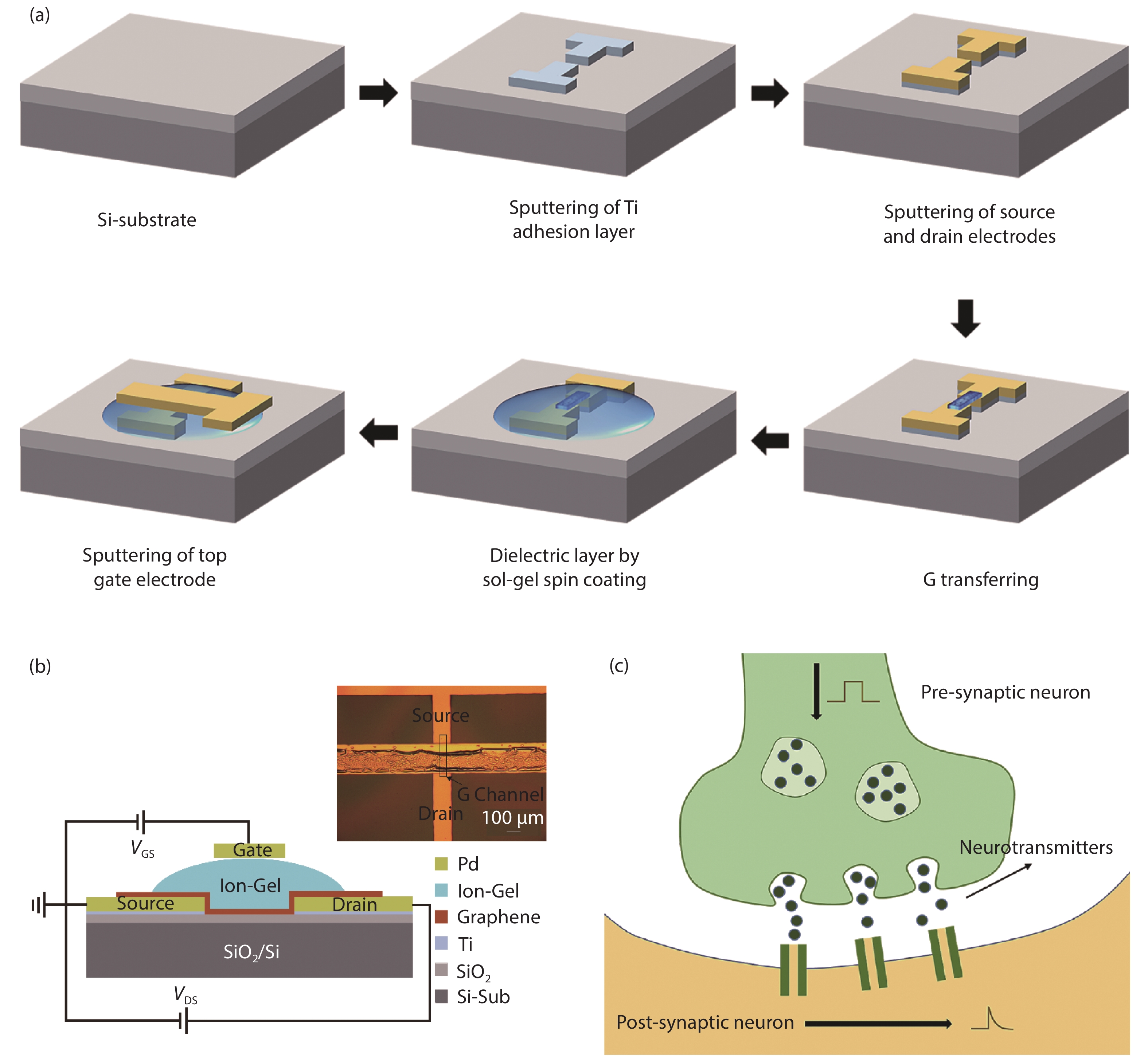
Fig. 1(a) shows the details of the process flow for the fabrication of multi-terminal graphene synaptic EDLTs. A silicon wafer with a 300 nm silicon dioxide (SiO2) layer was used as the substrate. Ti/Pd (5/100 nm) was deposited on the substrate using the magnetron sputtering method as the source and drain electrode, in which Ti is the adhesion layer. The graphene film was patterned by photolithography followed with oxygen plasma etching. The dielectric layer was formed by depositing the Ion-Gel onto the graphene channel with the spin coating process, first at 500 rpm for 15 s and then 3000 rpm for 45 s. Finally, the top-gate electrode was deposited.
![]()
Figure 1.(Color online) (a) An illustration of the process flow for the fabrication of graphene EDLTs. (b) Schematic and the top-view optical image of the graphene synaptic transistor. (c) Structure of the corresponding biological synapse.
2.4. Electrical measurements
The electrical performance of the graphene synaptic transistors was measured on a probe station with a semiconductor parameter characterization system (Agilent 4155C). Among all of our experiments, presynaptic spikes were applied on the top-gate electrode (with Keysight B2901) with VDS = 0.1 V.
3. Results and discussions
Fig. 1(b) shows the schematic and the related top-view optical image of the graphene synaptic transistor, where two metal electrodes are bridged by a graphene flake. The length of the graphene channel is ~70 μm. The top gate is coupled with the graphene channel by an Ion-Gel based dielectric layer. Surface irregularities are observed in the photo due to sputtering after spin coating the Ion-Gel gate dielectric.
The structure of the corresponding biological synapse is shown in Fig. 1(c). Stimulated by action potentials, neurotransmitters released from the presynaptic neuron[
In transistor-based artificial synaptic devices, the hysteresis behavior is typically used to indicate whether the device can emulate the basic function of the synapse[
![]()
Figure 2.(Color online) (a) Transfer curve (left) of the graphene transistor and the leakage current (right) through Ion-Gel. Fixed bias
As illustrated in Fig. 2(b), the typical potentiation behavior can be triggered by a presynaptic spike in our graphene synaptic transistors. ΔEPSC is the difference between the EPSC peak and the initial EPSC. A presynaptic spike (2 V, 100 ms) is applied on the top-gate electrode for the EPSC test, while the fixed drain bias VDS = 0.1 V is added as the readout voltage. By combing the results of the hysteresis behavior, the EPSC response to the spike input might be explained as follows: (1) The major carriers in the graphene channel are holes before a spike is applied (as shown in Fig. 3(a)). (2) With the application of a positive voltage of 2 V to the device, the anions in the Ion-Gel move toward the top and the cations toward the bottom. Meanwhile, the channel carriers become electrons because of the ambipolar conductive of graphene (as shown in Fig. 3(b)). Therefore, the hole concentration first decreases until the carriers become electrons, and then the electron concentration gradually increases. This process corresponds to the process of the current first decreasing and then increasing (as shown in Fig. 3(f)). (3) The EDL is formed (as shown in Fig. 3(c)). More electrons are generated in graphene because of the capacitive gating effect, some of which are captured into the traps in SiO2. (4) The concentration of electrons gradually reduces after the spike is removed. The initial sharp reduction is due to the rapid disappearance of electrons at high electron concentrations. Then the electron concentration decreases, while the cations at the bottom of the Ion-Gel diffuse slowly, so the reduction becomes slower. (5) The concentration of electrons decreases continually until a reversal occurs. The electron concentration is even lower than the initial hole concentration (as shown in Fig. 3(d)). Afterward, the concentration of holes increases. The captured electrons produce more holes in the channel than the initial state (as shown in Fig. 3(e)). This phenomenon represents potentiation behavior.
![]()
Figure 3.(Color online) The working mechanisms of the synaptic device under positive voltage. Charge distributions (a) before the pulse is applied, (b) when a positive voltage is just applied, (c) after applied spike stabilization, (d) when the spike is just removed, and (e) after removing the pulse for a while are shown respectively. (f) Drain current corresponding to the mechanism.
Fig. 4 shows the spike duration-dependent and the spike amplitude-dependent EPSCs of the graphene synaptic transistors separately. The ΔEPSC increased from ~50 to ~90 μA when the spike duration increased from 100 to 600 ms, as shown in the inset of Fig. 4(a). This happens because the longer spike duration leads to more mobile ions migrating to the graphene/Ion-Gel interface, resulting in a significant increase of the graphene conductivity. It can be seen that the ΔEPSC remains unsaturated when the spike duration is 600 ms, which might be related to a large number of movable ions in the Ion-Gel. As shown in Fig. 4(b), the changes of the presynaptic pulse amplitude make the ΔEPSC increase from ~7 to ~60 μA. This indicates that the postsynaptic responses are greatly influenced by the presynaptic stimuli including amplitude and duration[
![]()
Figure 4.(Color online) (a) EPSCs triggered by different spike duration for the same spike amplitude of 2 V are shown versus time. The spike duration increases from 100 to 600 ms. Inset: ΔEPSCs versus spike duration are plotted. (b) EPSCs triggered by different spike amplitude for the same spike duration of 100 ms are shown versus time. The spike amplitude increases from 0.5 to 3 V. Inset: ΔEPSCs versus spike amplitude are plotted.
In biological systems, PPF has an important effect on the reception and processing of information in the human brain[
![]()
Figure 5.(Color online) (a) A paired presynaptic spikes (2 V, 100 ms) with Δ
4. Conclusion
In conclusion, an Ion-Gel-coupled graphene synaptic transistor was demonstrated. The top gate and graphene channel can be considered as a presynaptic terminal and a postsynaptic terminal, respectively. The concentration and type of carriers in the graphene channel can be regulated by the EDL formed in the Ion-Gel dielectric layer. EPSC and PPF, which are basic mechanisms of synaptic STP, were successfully mimicked. In this artificial graphene synaptic transistor, the Ion-Gel layer itself possesses great flexibility, and the manufacturing processes are compatible with solution method, and the graphene also possesses very good flexibility. This work may be interesting for the application of graphene synaptic transistors in flexible electronics.
Acknowledgements
This work was supported by the National Natural Science Foundation of China (No. 61671368, 61172041).
References
[1] First draft of a report on the EDVAC. IEEE Ann Hist Comput, 15, 27(1993).
[3] The building blocks of a brain-inspired computer. Appl Phys Rev, 7, 11305(2020).
[4] et alFully hardware-implemented memristor convolutional neural network. Nature, 577, 641(2020).
[5] Towards spike-based machine intelligence with neuromorphic computing. Nature, 575, 607(2019).
[8]
[11] In-memory computing with resistive switching devices. Nat Electron, 1, 333(2018).
[19] Astrocytes gate Hebbian synaptic plasticity in the striatum. Nat Commun, 7, 13845(2016).
[28] et alEnhanced performance of graphene transistor with ion-gel top gate. Carbon, 68, 480(2014).
[30] et alGraphene synaptic transistor based on Ion-Gel dielectric. IEEE International Conference on Electron Devices and Solid-State Circuits, 1(2019).
[31] Short-term synaptic plasticity. Annu Rev Physiol, 64, 355(2002).
[32] Synaptic computation. Nature, 431, 796(2004).
[33] Metaplasticity: tuning synapses and networks for plasticity. Nat Rev Neurosci, 9, 387(2008).
[35] et alGraphene dynamic synapse with modulatable plasticity. Nano Lett, 15, 8013(2015).
[36] et alHysteresis of electronic transport in graphene transistors. Acs Nano, 4, 7221(2010).

Set citation alerts for the article
Please enter your email address
© Copyright 2018-2021 | Chinese Laser Press. All Rights Reserved 沪ICP备15018463号-20